CFP really shines at low bias current. My last MOSFET output DIY amp runs too hot as my like. This might be my next one.
The THD in simulation is about -100dB with 10KHz.
mosfets are used in the input stage and the VAS. I find they are just better than BJT in this context.

The THD in simulation is about -100dB with 10KHz.
mosfets are used in the input stage and the VAS. I find they are just better than BJT in this context.
Last edited:

If you change the output stage to darlington connection you ought to be able to decrease C3 and maybe take away C1+R11 and C2+R12. Faster amplifier = more open loop gain at 10kHz = lower distortion.
If you double R8+R9 the ideal idle current will be half as big. A few pF in paralell with R3 is usually also needed.
I think the difference is much bigger in the real world as in a simulation because the crossover distortion in sziklay pairs have to do with the switch off time in the output transistors. In darlington pairs the output transistors have much lower impedance to the base wich make them faster.
C7 is a smart thing reducing the thump in the loudspeakers at switch on. Have you checked what a current generator for the input pair will do? In a simulation the input transistors are identical but in the real world it can be difficult to find a pair with VGS closer than 50mv. Thats a thing to measure not to simulate but if you know how to change the VGS in a spice model...
It is remarkable how high gain a VAS with a Mosfet can have when it is driven from a current mirror.
The ZVP4424A lists a threshold voltage variation from -0.7 to -2.0V - that's risking producing serious DC-offset in a real amp built from them, and could even product current imbalance in the input pair. The high transconductance and low Vbe variation of bipolar's is what makes them great as a differential pair in many circumtances, especially with careful choice of emitter degeneration (typical variations in bipolars are ~50mV, much smaller than FETs).
Note that simulation doesn't show device-variation issues, and will thus hide this issue completely from you.
Your input network could be more robust to protect Q1 from ESD and RF. The input is DC-coupled and its a DC amp so I would worry that speaker damage might happen if the source is faulty, or clipping, or there is a poor ground connection to the source - one capacitor will fix that. Why not go for a conventional input network with DC-blocking, RF filtering, roofing filter and DC-blocking cap bleeder resistor. Tried and tested - its only 6 components, with the first RF cap mounted on the input connector (internal wires are often strong radiators for phone RF with its short wavelengths).

Since ZVP4424A is a high voltage switching MOSFET its noise performance is unknown - there's no requirement for a switching MOSFET to have low voltage noise or a low 1/f knee for voltage noise, so the process used may be poor for this - you'd have to do some research to find out how good/bad it is, but as its MOS I suspect its quite bad. Compare to for instance a KSA992 with perhaps 1dB noise figure at 1mA and 1k input impedance.
Also I would worry about gate protection on Q7, it would be easy to add a zener. Singleton MOS devices are very sensitive to ESD & stray electric fields, as typically they have no in-built gate protection (unlike CMOS ICs).
If you read the design analysis behind the Blameless amp you'll see its all based on actual measurement and every part is backed up by (many) distortion measurements on an Audio Precision analyzer - improving it takes a lot of careful analysis and real-world measurement, it can't be done by simulation alone. In particular the design decision to use bipolar input pair over JFET or MOSFET is quite reasoned and deliberate to achieve lower distortion and offsets and transistors are specifically chosen for low noise.
Note that simulation doesn't show device-variation issues, and will thus hide this issue completely from you.
Your input network could be more robust to protect Q1 from ESD and RF. The input is DC-coupled and its a DC amp so I would worry that speaker damage might happen if the source is faulty, or clipping, or there is a poor ground connection to the source - one capacitor will fix that. Why not go for a conventional input network with DC-blocking, RF filtering, roofing filter and DC-blocking cap bleeder resistor. Tried and tested - its only 6 components, with the first RF cap mounted on the input connector (internal wires are often strong radiators for phone RF with its short wavelengths).
Since ZVP4424A is a high voltage switching MOSFET its noise performance is unknown - there's no requirement for a switching MOSFET to have low voltage noise or a low 1/f knee for voltage noise, so the process used may be poor for this - you'd have to do some research to find out how good/bad it is, but as its MOS I suspect its quite bad. Compare to for instance a KSA992 with perhaps 1dB noise figure at 1mA and 1k input impedance.
Also I would worry about gate protection on Q7, it would be easy to add a zener. Singleton MOS devices are very sensitive to ESD & stray electric fields, as typically they have no in-built gate protection (unlike CMOS ICs).
If you read the design analysis behind the Blameless amp you'll see its all based on actual measurement and every part is backed up by (many) distortion measurements on an Audio Precision analyzer - improving it takes a lot of careful analysis and real-world measurement, it can't be done by simulation alone. In particular the design decision to use bipolar input pair over JFET or MOSFET is quite reasoned and deliberate to achieve lower distortion and offsets and transistors are specifically chosen for low noise.
The Cgd in mosfet is not linear. I want to use big enough miller cap to be dominant.If you change the output stage to darlington connection you ought to be able to decrease C3 and maybe take away C1+R11 and C2+R12. Faster amplifier = more open loop gain at 10kHz = lower distortion.
C1, R11, C2, R12, they are CFP parasitic oscillation snubbers. I have been working on this for quite awhile. The poles they introduced are very high. They are not concerned in general.
The loop gain bandwidth of this design is about 1MHz to 3MHz as I don’t really know the gm of the mosfet.
In my simulation, an optimal biased CFP is about 10dB lower 5W THD than an optimal biased EF2. You don’t need very much current to get optimal biased CFP. I found 20mA at the output devices is about right.I think the difference is much bigger in the real world as in a simulation because the crossover distortion in sziklay pairs have to do with the switch off time in the output transistors. In darlington pairs the output transistors have much lower impedance to the base wich make them faster.
I never measured the THD in real life though.
C7 is a smart thing reducing the thump in the loudspeakers at switch on. Have you checked what a current generator for the input pair will do? In a simulation the input transistors are identical but in the real world it can be difficult to find a pair with VGS closer than 50mv. Thats a thing to measure not to simulate but if you know how to change the VGS in a spice model...
It is remarkable how high gain a VAS with a Mosfet can have when it is driven from a current mirror.
This current source on VAS has NFB going on. It doesn’t need a big cap for filtering. The 0.1 here is just to prevent the parasitic oscillation from the NFB. I have done this in past. Yes, I can confirm that there is no thump or pop at powering on/off.
I expect there will be DC offset, but it should not be greater than 100mV. That’s why I omitted the input cap, as the DC offset from the mosfets presents at the output anyway.
I have these mosfets on hand. Usually they are close enough that it won’t be a concern for a speaker, but I will not use them in current mirror.
I looked at the scheme you posted with the bipolar output transistors. With MOS output transistors it will behave totally different in the high frequency area.
I have done numerous tests in real life where i tried to use FETs in rail to rail amplifiers. No one worked as I wanted. A main problem was that the G-S resistors had to be small with the following high current from the drivers in order to be able to switch off fast. But it was a lot easier to avoid self oscillations than with bipolar output. For IRF 540 + 9540 you need at least 30 mA and to me thats too much for the 10 w desktop amp i want.
In the Cordell book, designing audio power amps, you have good analyses why he used bipolar drivers in MOSFET ampliers.
You can download it for free.
As you said, there would be DC offset if the input pair is not matched. I figured the input cap wouldn’t do much for DC offset in this context. Thus, I left it out.Your input network could be more robust to protect Q1 from ESD and RF. The input is DC-coupled and its a DC amp so I would worry that speaker damage might happen if the source is faulty, or clipping, or there is a poor ground connection to the source - one capacitor will fix that.
BTW, is there any device that can measure the threshold voltage of the mosfet?
Yes, I have the “Handbook”.If you read the design analysis behind the Blameless amp you'll see its all based on actual measurement and every part is backed up by (many) distortion measurements on an Audio Precision analyzer - improving it takes a lot of careful analysis and real-world measurement, it can't be done by simulation alone. In particular the design decision to use bipolar input pair over JFET or MOSFET is quite reasoned and deliberate to achieve lower distortion and offsets and transistors are specifically chosen for low noise.
However, I don’t fully agree some of the points in the book.
For example, the input stage, if you single out the input stage, putting degenerative resistors makes it more linear but with lower gain. However, if you put the input stage within an amp, the distortion of the output stage always dominates, and the gain is more important so that you can use NFB. The linearity of the input stage doesn’t really matter. For me, I’ll just keep the degeneration minimal just to keep amp stable.
The biggest drawback of the BJT is that the input impedance would be projected to emitter. Let’s say the input impedance is 10K, the Beta is 200. It equivalent to additional 10K/200=50 Ohm degeneration at the emitter. It changes loop gain bandwidth while you moving the pot. For me, BJT input stage should not be a serious design nowadays.
JFET is a good and proven alternative. However, their lower voltage rating requires cascode for any acceptable power.
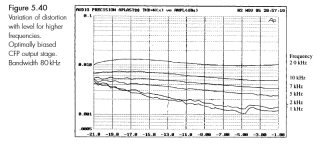
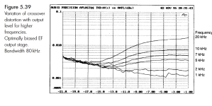
CFP has significantly higher THD at low power than an EF2.CFP really shines at low bias current
Attachments
Last edited:
Do you have link/reference?CFP has significantly higher THD at low power than an EF2.
I agree with your view of the input pair.
When i use TO92 mosfets i just measure them on a breadbord. I have 4,7k ohm to about 12v power supply and then shortcircuit D-G.
Multimeter breadboarded too. Plug in look at the DVM and put them in a row on a paper. Not the VGS for every single transistor and ready when 2 is close enough.
For SMD i use double transistors and hope.
We have a thread here of comparing distortion for different input transistor pairs. And surprisingly the Mosfets were the best.
Many professional amplifiers use Mosfet input today but with a DC servo to minimise output DC. They are much better at RFI.
In my experience the darlington connection is much better in the real life. Especially when you look at crossover distortion.
I dont think the softwares handles the crossover region correctly as it is so far away from transistors conducting at DC.
CFP needs extra care with the parasitic oscillation. https://www.diyaudio.com/community/...tor-with-emitter-follower.421436/post-7885967I looked at the scheme you posted with the bipolar output transistors. With MOS output transistors it will behave totally different in the high frequency area.
I have done numerous tests in real life where i tried to use FETs in rail to rail amplifiers. No one worked as I wanted. A main problem was that the G-S resistors had to be small with the following high current from the drivers in order to be able to switch off fast. But it was a lot easier to avoid self oscillations than with bipolar output. For IRF 540 + 9540 you need at least 30 mA and to me thats too much for the 10 w desktop amp i want.
In the Cordell book, designing audio power amps, you have good analyses why he used bipolar drivers in MOSFET ampliers.
You can download it for free.
Are you talking about CFP with BJT driver and MOSFET output? It is in the same situation. They also have very high gm overall.
I just edited my post with D. Self comparisons.Do you have link/reference?
There are many differencies in the behaviour with MOSFETs as the output transistors.
First of all the mosfet is much faster if you exclude the input capacitance.
And if i understand them right the input capacitance works the same whether the current is very small or large. Or increasing - decreasing.
The bipolars are much more complicated. The speed - Ft varies a lot with the current and switching on and off are different. And many times they rectifie
input signal because the base conducts more and more the greater the current is.
I am surprised to see Douglas Selfs comparition of the output stages. In my memory ( i left szikay pairs in the 1970:s) the difference was 5 or 10 times.
Maybe he tested with faster output transistors?
Here is the thread comparing input transistors,
People always talk about JFET in the input stage, but nobody talk about using MOSFET in the input stage.
The only reason that I could find is MOSFETs have high noise figure. How high is too high? Does it matter in the power amplification context? It is not a preamp.
As JFETs are pretty delicate, the voltage rating is pretty low. You have to babysit them. In contrast, you can find MOSFETs with voltage rating from 60v to 240v in TO-92 package easily.
In my simulation, BS170 is more linear, lower distortion, higher transconductance than 2SK170. Why don't we use MOSFET?
- jxdking
- Replies: 26
- Forum: Solid State
I do have the book. Just read through that portion again.CFP has significantly higher THD at low power than an EF2.
Note that the optimal bias for EF2 is about 100mA, with 0.22Re, For CFP, it is about 11mA.
Thus, at -16dB Watt, EF2 is in pure class A. You see everything converges to the noise floor before -16dB. Can we over bias CFP? In general, no, it exhibits more distortion if you over bias CFP as it widens the crossover region.
Yes, CFP do have slightly higher distortion around 1W based on the book. I think it is a good trade off to have a cooler amp.
Last edited:
How does the phase margin look?
My Blameless attempt has a phase margin of 90 degrees over the audio spectrum which is overdamped resulting in poor transients if we take 60 ~ 75 as the best range...
My Blameless attempt has a phase margin of 90 degrees over the audio spectrum which is overdamped resulting in poor transients if we take 60 ~ 75 as the best range...
The loop gain bandwidth is about 2MHz with 105 degrees phase shift.How does the phase margin look?
My Blameless attempt has a phase margin of 90 degrees over the audio spectrum which is overdamped resulting in poor transients if we take 60 ~ 75 as the best range...
The original Blameless limits the loop gain bandwidth around 600KHz. With modern 30MHz output transistors, such as 2SC5200/2SA1943, it is too conservative. As you said, it is overdamped in most cases. That's one of the reason I want to promote to use fast devices and set loop gain bandwidth around 2MHz to 3MHz for modern design.
- Home
- Amplifiers
- Solid State
- Modernize The Blameless, And The CFP