I'm thinking about using an optoisolator as a way to stabilize the bias current in an audio amplifier, VERY similarly to Nelson Pass's 26-year-old patent, number 4752745, attached below. I'm considering the "4N35" optoisolator, so I thought I'd buy ten of them from two different manufacturers and measure them. Datasheets tell you what you MIGHT get, measurements tell you what you DID get (this time anyway).
To my delight I found that the Lite-ON part and the Vishay part, performed about the same. And, the variance was not terribly large. I'm sure if I tested ten thousand 4N35s from twenty different fab lots spread across three years' worth of production, the variance would be larger. But that is another discussion for another day. These are the parts I have in hand today, and this is how they behave.
To my delight I found that the Lite-ON part and the Vishay part, performed about the same. And, the variance was not terribly large. I'm sure if I tested ten thousand 4N35s from twenty different fab lots spread across three years' worth of production, the variance would be larger. But that is another discussion for another day. These are the parts I have in hand today, and this is how they behave.
Code:
4N35 OPTOISOLATOR
BASE UNCONNECTED (FLOATING)
EMITTER FOLLOWER CONFIG
COLLECTOR = +10V
100R EMITTER RESISTOR TO GND


UNIT  MFR       VLED@10mA   ICE(mA)
-----------------------------------
  1   LITE-ON     1.179      28.4
  2   LITE-ON     1.186      19.3
  3   LITE-ON     1.181      19.1
  4   LITE-ON     1.173      27.6
  5   LITE-ON     1.178      25.5
  6   LITE-ON     1.173      28.2
  7   LITE-ON     1.175      24.1
  8   LITE-ON     1.173      26.8
  9   LITE-ON     1.177      19.5
 10   LITE-ON     1.175      23.1

 11   VISHAY      1.186      27.6
 12   VISHAY      1.186      29.0
 13   VISHAY      1.186      26.5
 14   VISHAY      1.187      25.9
 15   VISHAY      1.186      27.6
 16   VISHAY      1.186      27.8
 17   VISHAY      1.187      25.4
 18   VISHAY      1.185      29.3
 19   VISHAY      1.187      25.6
 20   VISHAY      1.186      27.0
Attachments
One bit of warning -- don't use these in low-level stages or driving high impedances as they have very high noise. I tried using them as a remote-controlled current source in an amp circuit (in high impedance, not bypassed) and they hissed like crazy. I guess that's what you get when the base circuit of a bjt is effectively open.
Bwaslo, thanks very much for the tip! Current thought is to connect mondo capacitance from emitter to collector since the output side is supposed to act as a low impedance "bias spreader" (voltage source).
Wondering Mark, if you are familiar with Edmond Stuart's auto bias article, not sure if it is similar in any way to what you are doing. Is yours for output stage biasing?
http://www.diyaudio.com/forums/solid-state/145013-variable-operating-biass-output.html#post2209540
Here it is on the wayback machine:
https://web.archive.org/web/20100729011121/http://home.tiscali.nl/data.odyssey/AutoBias.html
http://www.diyaudio.com/forums/solid-state/145013-variable-operating-biass-output.html#post2209540
Here it is on the wayback machine:
https://web.archive.org/web/20100729011121/http://home.tiscali.nl/data.odyssey/AutoBias.html
I'm going to try something similar to Nelson Pass's patent, which is different from Edmond Stuart's article in that (a) it uses one optoisolator rather than two; and (b) it doesn't require two matched-pairs of transistors and three matched resistors. I am happy to forefit the additional distortion reductions, which the extra complexity is claimed to provide.
I'm thinking about using the 4N35 to "servo" the voltage across the output transistors' emitter resistors / source resistors. If this voltage stays constant then the current through those resistors also stays constant, which means the output stage bias current is constant.
Depending upon whether the output stage is a double or a triple, and depending upon whether the transistors are MOSFETs or BJTs, the bias spreader voltage (= optoisolator VCE) could be as low as 2.4 volts, and it could be as high as 12 volts. So I decided to measure the 4N35 at a variety of VCE voltages, and find out whether it misbehaves at some or all VCEs.
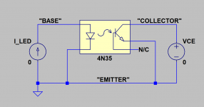
If we ground the cathode of the input (LED) side, and if we also ground the emitter of the output (phototransistor) side, then the optoisolator behaves as an NPN transistor with unusually low beta. See Figure 1 below. I connected it this way and plugged it into my curve tracer, set to measure NPN transistors.
My results are in Figure 2 below. The raw data (excel spreadsheet) is included in a .zip archive, if you want to examine it more closely. {when you zoom in you'll see a certain amount noise in the measured data, which is not so visible in the zoomed-out figure here}.
For me the big surprise is that the phototransistor shows a degree of quasi-saturation at high current and low voltage. If I want to run it at low VCE, I had better stay below ~ 12mA to 15mA of ICE, to keep away from quasi-saturation.
Early voltage is about 100 volts which is much higher than I dared to expect.
The spacing between the curves is relatively constant, which means the "Beta" of this NPN {optoisolator datasheets call it the "Current Transfer Ratio"} is also relatively constant, at about 2.5 or so.
_
Depending upon whether the output stage is a double or a triple, and depending upon whether the transistors are MOSFETs or BJTs, the bias spreader voltage (= optoisolator VCE) could be as low as 2.4 volts, and it could be as high as 12 volts. So I decided to measure the 4N35 at a variety of VCE voltages, and find out whether it misbehaves at some or all VCEs.
If we ground the cathode of the input (LED) side, and if we also ground the emitter of the output (phototransistor) side, then the optoisolator behaves as an NPN transistor with unusually low beta. See Figure 1 below. I connected it this way and plugged it into my curve tracer, set to measure NPN transistors.
My results are in Figure 2 below. The raw data (excel spreadsheet) is included in a .zip archive, if you want to examine it more closely. {when you zoom in you'll see a certain amount noise in the measured data, which is not so visible in the zoomed-out figure here}.
For me the big surprise is that the phototransistor shows a degree of quasi-saturation at high current and low voltage. If I want to run it at low VCE, I had better stay below ~ 12mA to 15mA of ICE, to keep away from quasi-saturation.
Early voltage is about 100 volts which is much higher than I dared to expect.
The spacing between the curves is relatively constant, which means the "Beta" of this NPN {optoisolator datasheets call it the "Current Transfer Ratio"} is also relatively constant, at about 2.5 or so.
_
Attachments

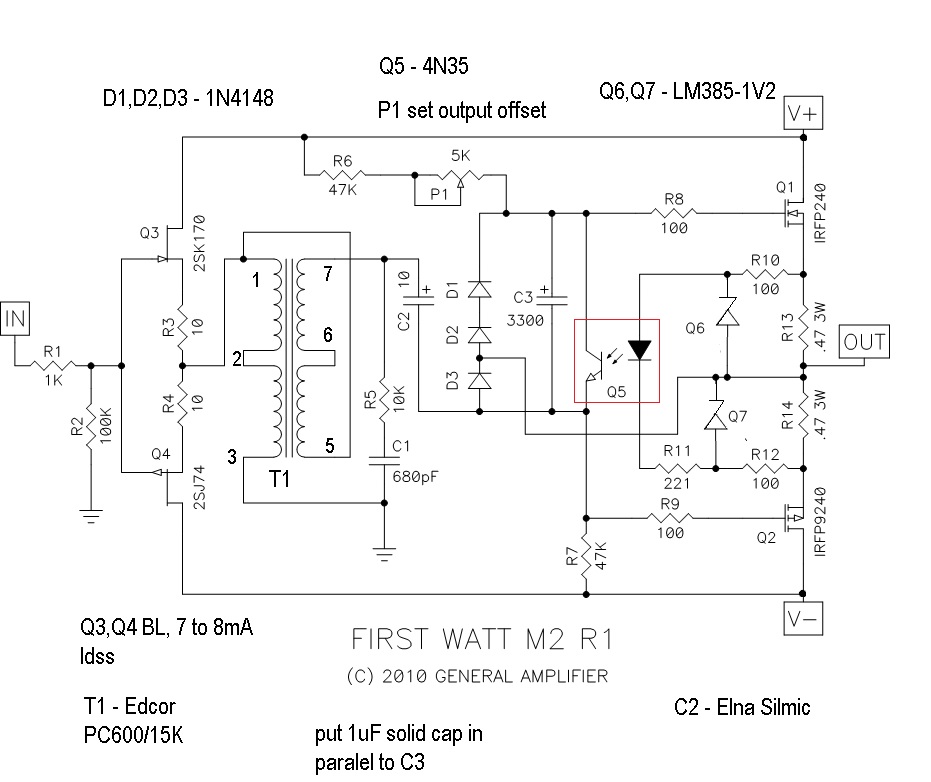
I built a Pass M2 that uses the 4N35 in the bias circuit. It works very well. Rock stable bias circuit. With a 3300uF cap, it has a slow start feature that is cool as it starts at low bias and gradually (over a minute) rises to class A. You can hear the difference as the bias rises.
ZM did a ncie job explaining it here:
http://www.diyaudio.com/forums/pass-labs/281520-official-m2-schematic-163.html#post4924962
I have always wanted to try on a different amp.
ZM did a ncie job explaining it here:
http://www.diyaudio.com/forums/pass-labs/281520-official-m2-schematic-163.html#post4924962
I have always wanted to try on a different amp.
The Pass M2 is certainly not in any danger of quasi-saturation; he's running the phototransistor at about 400 microamps of ICE.
Math: [(|VCC| + |VEE|) - (|Vgs1| + |Vgs2| + VLED)] / (R6 + R7) = 0.00039 amps
Math: [(|VCC| + |VEE|) - (|Vgs1| + |Vgs2| + VLED)] / (R6 + R7) = 0.00039 amps
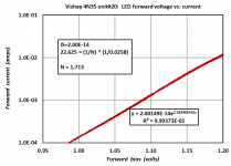
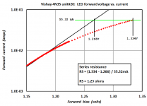
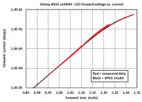
Measuring the (exponentially!) nonlinear I-V behavior of the 4N35's input side, namely, the LED.
As shown in Figure 1, there is a kink at Vin=1.03 volts; the slope changes visibly. SPICE's equations do not provide for this, so any fitted model will be a compromise. Figures 2-4 show the compromises that I decided to make.
_
As shown in Figure 1, there is a kink at Vin=1.03 volts; the slope changes visibly. SPICE's equations do not provide for this, so any fitted model will be a compromise. Figures 2-4 show the compromises that I decided to make.
_
Attachments

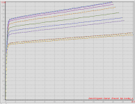
Next I took a look at the variability of 4N35 behavior, from unit to unit. The Vishay devices seemed more tightly grouped than the LiteON devices, so I decided to further investigate the LiteON parts.
I plotted Iout versus VCE for several LiteON 4N35s, with a constant LED input current of 5.0mA in every case: see attached image. The current transfer ratio (CTR = Iout/Iin) varied from 1.50X to 2.26X. The geometric mean of the extremes is 1.84X and the extremes are displaced ±23% from the mean. Conservative design-for-yield would require correct functionality far beyond the limits of this modest dataset; perhaps ±40% or ±50% from the mean. Wow.
_
Attachments
the transistor output opto CTR is directly hfe dependent
its usually considered a poor design choice to depend on hfe given device spreads and TC
optos in regulating loops usually have other sense/feedback paths and are really only used for the isolation given the isolated path uncertain current gain
more circuitry is required with the tiny direct base photo current being O 1k less than the LED current but it should be very stable compared to hfe
for accurate optoisolation HCNR200 uses 2 photo diodes and has one on the LED side to monitor the actual light output to compensate for LED sensitivies, aging
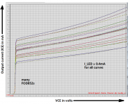
I realized I had a tube of Darlington optoisolators, Fairchild FOD852s, so I put those on the tester too.
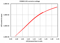
As shown in image 1, these LEDs seem to "turn on" at slightly lower voltage: 1.1V or so, rather than the 1.2V of the 4N35s.
Image 2 treats the optoisolator as a weird NPN transistor: "base current" (actually: LED current) is stepped from 0.3mA to 0.55mA, while collector voltage is swept. Collector current is plotted on the Y axis. Again we see a whiff of quasi-saturation, at low VCE and high ICE.
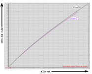
I fixed the LED current at 0.4mA and tested a bunch of different FOD852 parts, overlaying the I-V curves on a single plot, to get an idea of their variability. The result was Image 3. Current Transfer Ratio (= ICE / ILED) varied from about 20X to 38X.
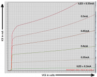
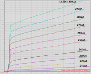
The curve tracer has a cool feature that lets you plot Beta versus collector current; I enabled that feature and instead got a plot of Current Transfer Ratio versus output current, in Image 4. The damn thing just gets better and better as you crank up the current. But my intended application (as a bias spreader in an audio amplifier) will run the optoisolator at relatively low currents. So I adjusted the settings to keep the entire plot within (0 < ICE < 8mA) and the result is Image 5. Notice that at very low collector currents, the CTR falls precipitously. Yikes.
_
As shown in image 1, these LEDs seem to "turn on" at slightly lower voltage: 1.1V or so, rather than the 1.2V of the 4N35s.
Image 2 treats the optoisolator as a weird NPN transistor: "base current" (actually: LED current) is stepped from 0.3mA to 0.55mA, while collector voltage is swept. Collector current is plotted on the Y axis. Again we see a whiff of quasi-saturation, at low VCE and high ICE.
I fixed the LED current at 0.4mA and tested a bunch of different FOD852 parts, overlaying the I-V curves on a single plot, to get an idea of their variability. The result was Image 3. Current Transfer Ratio (= ICE / ILED) varied from about 20X to 38X.
The curve tracer has a cool feature that lets you plot Beta versus collector current; I enabled that feature and instead got a plot of Current Transfer Ratio versus output current, in Image 4. The damn thing just gets better and better as you crank up the current. But my intended application (as a bias spreader in an audio amplifier) will run the optoisolator at relatively low currents. So I adjusted the settings to keep the entire plot within (0 < ICE < 8mA) and the result is Image 5. Notice that at very low collector currents, the CTR falls precipitously. Yikes.
_
Attachments

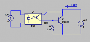
Those integrated-Darlington optoisolators seemed awfully anemic at low currents where I intend to operate in an audio amplifier bias application. I wanted a lot of gain in the neighborhood of (2.5mA < Iout < 10mA) so I experimented with an external discrete transistor (PN2222) as a current booster: see image 1 below.
This increased the Current Transfer Ratio quite a bit, in the low current zone where I plan to operate. As shown in image 2, 250 uA input produces 5 mA output at VCE=2.5 volts, and slight increases in input current give large increases in output current. So the DC bias feedback loop will have plenty of gain, just as I desire. And of course there's another factor of 3X gain available if I switch to a superbeta transistor instead of the junkbox 2222.
This increased the Current Transfer Ratio quite a bit, in the low current zone where I plan to operate. As shown in image 2, 250 uA input produces 5 mA output at VCE=2.5 volts, and slight increases in input current give large increases in output current. So the DC bias feedback loop will have plenty of gain, just as I desire. And of course there's another factor of 3X gain available if I switch to a superbeta transistor instead of the junkbox 2222.
Attachments
- Status
- Not open for further replies.
- Home
- Amplifiers
- Solid State
- Measuring & modeling 4N35 optoisolators for Optical Bias amplifier uses