I've been playing around with some CD4000 series, medium current, unbuffered inverters, part number CD4049UB. Generally people use a different part, the low current unbuffered inverter (4069), to build quartz crystal oscillators and such, because low current protects the crystal from heating if the circuit design is sloppy. But I wanted to experiment with the medium current device (4049) instead. Its datasheet is attached below.
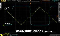
I measured its Vin versus Vout characteristic, it's shown in Figure 1 below. A very slow (100 Hz) triangle wave is applied to the input, and the output waveform is captured. The picture shows that it only takes a very small change on the CD4049UB input, to swing the output from rail to rail. The gain is pretty high.
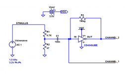
So I built the little test jig shown in Figure 2, on my solderless breadboard. A 100-to-1 voltage divider creates very small amplitude sinewaves, which are AC coupled to the inverter input. Resistor R3 biases the inverter at the point where Vin=Vout, the point where the yellow trace crosses the blue trace in Figure 1. This is in the steep-slope (high gain) region.
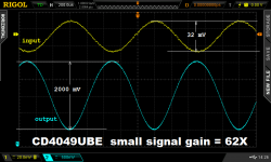
Results are shown in Figure 3. I dialled the input amplitude down until the output signal was a 2 volt peak-to-peak sinewave. This is comfortably far away from clipping / hitting the rails, so the amplifier is operating in its most linear region. As you can see, it took 32mV of input amplitude to produce 2 volts of output amplitude; the gain was 62.5X. Not bad for a "digital" component.
_
I measured its Vin versus Vout characteristic, it's shown in Figure 1 below. A very slow (100 Hz) triangle wave is applied to the input, and the output waveform is captured. The picture shows that it only takes a very small change on the CD4049UB input, to swing the output from rail to rail. The gain is pretty high.
So I built the little test jig shown in Figure 2, on my solderless breadboard. A 100-to-1 voltage divider creates very small amplitude sinewaves, which are AC coupled to the inverter input. Resistor R3 biases the inverter at the point where Vin=Vout, the point where the yellow trace crosses the blue trace in Figure 1. This is in the steep-slope (high gain) region.
Results are shown in Figure 3. I dialled the input amplitude down until the output signal was a 2 volt peak-to-peak sinewave. This is comfortably far away from clipping / hitting the rails, so the amplifier is operating in its most linear region. As you can see, it took 32mV of input amplitude to produce 2 volts of output amplitude; the gain was 62.5X. Not bad for a "digital" component.
_
Attachments
> gain was 62.5X
There's an old-old RCA paper, now branded Fairchild but curated by ON Semi.
https://www.fairchildsemi.com/application-notes/AN/AN-88.pdf
Page 3 says at 5V supply the gain is 40dB, 100X, well within sight of your 62.5X considering all the process-change since 197? and that this performance is not on the datasheet; and you tried 4049 not 74C04.
Any sign of cross-conduction currents (from the power supply) at the switching point? Curious about the magnitude of these.
The datasheet promises that at room temperature, with a 5V power supply, the CD4049UB's max(IOL, IOH) is only 6.4 mA. So cross-conduction {CMOS IC designers call it "crowbar" and/or "shoot-through"} currents are going to be small and quite manageable.
When wiring my test jig, I connected a 100 ohm resistor from VCC to GND, to establish a baseline load upon the benchtop powersupply. This sets Iout to 50mA, so the PSU's output pass transistor is running at decent current, thus the gm of the pass transistor is reasonably high. I figured that 6 or 7 mA of variation, riding on top of 50 mA DC current, would produce negligible ripple.
Then as a further precaution, I added ten or twelve multilayer ceramic bypass capacitors, up and down the supply rails of the solderless breadboard. Now the voltage regulator inside the benchtop power supply handles the low frequency components of Iout, and the bypass caps handle the high frequency components. It worked in the lab, as predicted on the chalkboard: beautifully.
Of course anybody could replicate these experiments themselves; it's only a single IC and a couple ordinary pieces of test equipment. Lash it together and start investigating! You'll have results in less than two hours.
My eye says about 2% distortion so that's not bad for something so simple.
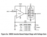
Yes, and you can enclose them in an NFB loop to reduce the distortion quite dramatically. Here's a figure from Linear Technology's application note AN-18, "Power Gain Stages for Monolithic Amplifiers".
_
Attachments
Attachments
Last edited:
- Status
- Not open for further replies.
- Home
- Amplifiers
- Solid State
- Measured: small signal gain of CMOS inverter logic gate. 62X!