Hi,
I am very appreciative of the artistic content of your layout but I'm afraid it will be an EMI inferno.
Contrary to what's typically believed, you should never cut up the ground plane (like is done on your board with the output filter caps). The ground plane should be one solid area with preferably no traces through it and no slots or cuts. Every slot will increase loop inductance and may even act as a "slot antenna".
Slots are often made in a vain attempt to control common-leg coupling of signals. The point is - if you arrange the layout such that no return current needs to flow in a sensitive circuit area, it won't!
Here's the algorithm for good PCB design:
Arrange ALL connectors together on one edge of the PCB. Do NOT make flow-through layouts where input is on one side and output is on the other (reason: you must provide HF decoupling to a single point. There will be a voltage across the ground plane and wires attaching to opposing sides will act like a dipole antenna with an HF voltage source between in the middle!)
It means you will have to arrange "U" shaped signal flows.
Allocate one PCB layer to ground. If you are making a two-layer board, make a 1-layer layout with only the ground connections on the other layer. Short "jump tracks" (<1cm near the power stages, <2cm elsewhere) are acceptable.
Use differential signalling (=kelvin sensing).
All filter caps should be close to the output connectors (which are on the same edge as the input connectors!). The coils should be closest to the power stages. If it so happens that the track between the coil and the filter cap becomes long: this is NOT a problem!
I know that these rules are very difficult to follow, but they are the ONLY way to obtain good EMI. Anything else, for whatever excuse one may imagine, is plainly incorrect.
You may find that these rules produce particular problems with ground-referenced signaling. Adopt differential (kelvin sensing) signaling throughout. This does not mean you need a balanced signal, but that you need to have a differential input.
Cheers,
Bruno
Bruno, my hat's off to you again.Bruno Putzeys said:Hi,
I am very appreciative of the artistic content of your layout but I'm afraid it will be an EMI inferno.
Contrary to what's typically believed, you should never cut up the ground plane (like is done on your board with the output filter caps). The ground plane should be one solid area with preferably no traces through it and no slots or cuts. Every slot will increase loop inductance and may even act as a "slot antenna".
Slots are often made in a vain attempt to control common-leg coupling of signals. The point is - if you arrange the layout such that no return current needs to flow in a sensitive circuit area, it won't!
Here's the algorithm for good PCB design:
Arrange ALL connectors together on one edge of the PCB. Do NOT make flow-through layouts where input is on one side and output is on the other (reason: you must provide HF decoupling to a single point. There will be a voltage across the ground plane and wires attaching to opposing sides will act like a dipole antenna with an HF voltage source between in the middle!)
It means you will have to arrange "U" shaped signal flows.
Allocate one PCB layer to ground. If you are making a two-layer board, make a 1-layer layout with only the ground connections on the other layer. Short "jump tracks" (<1cm near the power stages, <2cm elsewhere) are acceptable.
Use differential signaling (=kelvin sensing).
All filter caps should be close to the output connectors (which are on the same edge as the input connectors!). The coils should be closest to the power stages. If it so happens that the track between the coil and the filter cap becomes long: this is NOT a problem!
I know that these rules are very difficult to follow, but they are the ONLY way to obtain good EMI. Anything else, for whatever excuse one may imagine, is plainly incorrect.
You may find that these rules produce particular problems with ground-referenced signaling. Adopt differential (kelvin sensing) signaling throughout. This does not mean you need a balanced signal, but that you need to have a differential input.
 Completely agree with your message.
About the integrity of the ground plane, one should not be afraid of adding extra vias in order to minimize the length of the "jumpers" on that side. Avoid the temptation to extend a ground side jumper trace to bridge non adjacent signal traces. Even if a run must jump from side to side several times like stitch work, it is worth it. Also, sharing ground vias among components can sometime be problematic due to common impedance.
I strongly agree that all power handling connections should generally be grouped together, although one can sometimes do things like dedicate an edge of the PCB to become a "flat cable" in order to remotely locate a power connector for packaging reasons. The flat cable edge section must power over return and not touch the rest of the layout (kind of as if it were a cable draped along that edge). If any board side jumps are made in high current runs, an appropriate number of multiple vias must be used.
Also, signal connectors can be just about anywhere as long as the signals are at least quasi differential in nature.
I have a layout question for you, Bruno. How do you handle the congestion in the vicinity of the output mosfet bridge with only a two sided layout? There you have power, ground, two outputs, and the gate drives plus their returns and maybe some current sense signals. It's a real signal flow traffic jam! Do you use jumpers, extra layers, put the gate drive on daughter boards, or what? I never found a solution that I and the bean counters were simultaneously satisfied with.
Maybe I just didn't educate them well enough.

Regards -- analog(spiceman)
thank you,I think you are wonderful🙂
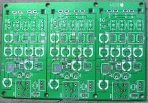
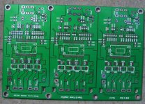
for rwagter,this is the chip M615171AFP that I used.
it is a all in one,2 channel 100W amp module.including drive stage and output stage.
regards
digi
for rwagter,this is the chip M615171AFP that I used.
it is a all in one,2 channel 100W amp module.including drive stage and output stage.
regards
digi
I spend inordinate amounts of time puzzling.analogspiceman said:
I have a layout question for you, Bruno. How do you handle the congestion in the vicinity of the output mosfet bridge with only a two sided layout? There you have power, ground, two outputs, and the gate drives plus their returns and maybe some current sense signals. It's a real signal flow traffic jam! Do you use jumpers, extra layers, put the gate drive on daughter boards, or what?
The UcD layout was in its 5th or 6th "generation" before it was finally ready to be used in production.
Nevertheless it's been a surprise how well ferrite beads and sense resistors etc consistently conspire to land just in the right place to run tracks under them. For boards handling serious currents (20A and up) I no longer manage with two-layer boards and I move up to 4 layers. Not that this makes life so much easier. Current-carrying tracks on the inner layers have to be made nearly 4 times as wide...
I start my layouts by placing the power MOSFETs, decoupling caps and the power inductor first. The power FETs go back-to back with the heatsink in-between. This to the frustration of bean counters because there is no standard "clip" mounting method for b2b TO220 devices.
This placement was originally chosen to allow the two current loops (top fet on or bottom fet on) to be laid out to have the same area and orientation. It then turned out to make life much easier running the supply tracks as well.
Next come the "gate off" transistors, then the rest (gate drivers are discrete, which makes them a bit more flexible to mould round the rest of the circuit).
Next come the "gate off" transistors
Brothers in arms - We fight the same battle!

Hehe, Bruno is probably going to pull out his hair in frustration when I post the layout for the front audio channel PCB for my preamp (but that should take at least a week more, if not more) 😀.
- Status
- Not open for further replies.
- Home
- Amplifiers
- Class D
- M61571AFP,50W 5.1ch CLASS D mini amp projects