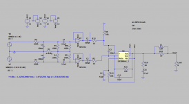
I am having hard time simulating a schematics - sometimes it shows DC offset at the load, and sometimes it does not. I am confused as to why LTSpice is not consistent with the simulation calculation.
I have tried a circuit with DC blocking capacitor and then without. And I am getting mixed results running one or another scenario multiple times. When I put together simulation first time I did not use DC blocking capacitor and when I measured load voltage, it started from strictly 0. Now, it is offset by -37mV.
When I include DC blocking capacitor, DC offset is -4.5mV.
I guess my question is - can I avoid using DC blocking capacitor?
Can someone help me with this? I am attaching schematics file with model files for both amps.
Thanks,
Pavlo