Having been intrigued by the Quad current dumping amps for several years now (but never built/listened to one) I recently dug out all the schematics and articles I collected over time and now want to give it a try in the real world. Not being content with buying a clone kit from eBay, I played around with LTspice and eventually arrived at a modified design that suits my parts bin.
- Started out with Keith Snook's DCD-3 schematic and adjusted it for 18V rails. Opamp can be powered directly from the rails now, BC550/560 are useable (45V VCE) and even 12VAC toroids may come to use here (albeit not reaching the full 18V). Reduced the opamp stage gain a little and resized the caps to 470nF, because PP caps are pretty bulky.
- Replaced R30/R31 of the dcd-schematic with a current source. Main advantage being that I now have another transistor that can be mounted to the heatsink to get rid of the heat, instead of having two concrete monsters that slowly burn holes into the pcb. I don't like hot resistors 😉. Another good thing is that the bias current for the Class A stage is now easily adjustable with a single resistor (don't use a potentiometer!). 12R is fairly close to the original 50mA, while two 10R in parallel will yield around 120mA. This should keep the dumpers off for a little longer. Of course idle dissipation will be higher, but the Class A transistor should handle that just fine due to the reduced supply voltage.
- One thing I'm not sure about is the use of D2 and D3 (D5 and D13 in the dcd-3 schematic). With the diodes fitted and a small signal or a light load applied, the whole output current seems to be delivered by the lower dumper while the upper one is turned off. Removing the two diodes balances the current about equal between the two dumpers. The diodes were probably deliberately chosen to achieve this, but why? I thought the theory was that the Class A stage should supply small currents to the load, being supported by the dumpers only for the heavier currents. In my simulation the Class A stage seems to be only delivering any substantial current to the load when I disconnect the dumper stage from the bridge altogether 😕.
Attachments
Interesting question, in the original 405, D1 was omitted and the base of Q1 and Q3 were directly connected so there is no output stage bias. D3 and D4 appear to bias the stage away from the output of the Class A stage, Q4 and Q5 collectors. This allows the output of the class A amplifier to drive the load through R7 and L2. When the class A amp drives more than 12mA into the load this will bias on the output stage. Without D2 and D3 the class A stage will drive the output stage directly and the feedforward arrangement will not work. With D1 fitted there is still no output stage bias and the class A stage will provide greater current to the load before the output stage is turned on. I am not sure of the need for R5
Stuart
Stuart
I am not sure of the need for R5
As a base stopper it probably doesn't harm either in that place.
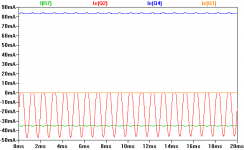
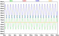
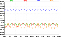
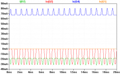
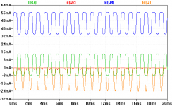
Here're some graphs that show the behaviour with and without the two diodes at a light load. Red and Orange are the emitter currents of the dumpers Q1 and Q2, Green is the current through R7 (which should be the Class A current driving the load) and Blue is the emitter current of the Class A stage transistor Q4.
First image shows the standard configuration. Almost all of the current is delivered by the lower dumper Q2, while the Class A stage remains basically quiescent.
Second image shows the dumpers disconnected from the bridge at the 500R/3uH point. Now the dumpers are both shut off and Q4 does all the work, delivering the current through R7.
Third image shows the dumpers reconnected again, but D2 and D3 shorted out. Now the current is shared much more equal between Q1 and Q2, while a small part (albeit being somewhat distorted) is contributed by the Class A stage. Since my understanding of the concept is still somewhat limited, I'm not sure how to interpret this results.
Attachments
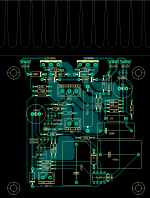
Here's a first layout iteration. Dimensions are 10x10cm. Power transistors were spaced for easy bolting to the heatsink (no screws right behind the fins). Plenty of board space for polypropylene capacitors. Added the opamp's zener diodes back in so they can be fitted for higher rail voltages. BC's can be substituted by 2N5551 and 2N5401 for higher rail voltages, simply rotate them by 180 degrees.
Attachments
- Status
- Not open for further replies.