Do we get to see the schematic?
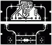
Have a look at the route the fast transient currents must follow into and out of the HF decoupling as they pass from Output PIN to output Zobel and back again.
With a route that long, can any fast transients pass around the loops?
Have a look at the route the fast transient currents must follow into and out of the HF decoupling as they pass from Output PIN to output Zobel and back again.
With a route that long, can any fast transients pass around the loops?
Do we get to see the schematic?
Input Cap not added, assume can be fitted at crossover output.
Zobel not added.
Attachments
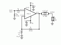
The schematic shows Cs.
You have placed the four Cs capacitors on the PCB, but in the wrong place.
The fast film or ceramic parts of Cs must be at the power pins and must be connected together in the shortest loop possible. The junction so formed is then connected to the corresponding junction of the electrolytic Cs. This common junction for all four Cs caps must be close to the OUTPUT PIN of the amplifier. Now connect the XZobel from OUT to Cs.
That is the ONLY way to allow the very fast rising and falling transients to pass around the Cs decoupling routes. Your decoupling route goes around the outside perimeter of the PCB and is about 10 (ten) times too long to be effective. The added inductance very effectively prevents the fast transients getting to their destination. In addition you have enclosed all the low level signal traces and components INSIDE the loops carrying those output currents. That makes for a good transmitter and receiver of unwanted distortions.
Start again.
Last edited:
There are many Threads where Members ask how to layout amplifiers.
Go and read and if you agree then adopt the ideas that suit you.
Go and read and if you agree then adopt the ideas that suit you.
You still have the decoupling capacitors connected by a long route that passes around the whole PCB. That route can never be short !!!!!!!!!!!!
Infact, Post # 4 is well descriptive, I read several times to understand what you want to say. Being not an electronics man, I understood few of them.
I tried to copy the style of "LM4780 SS Pcb" which appreciated by many members. My layout may be looks like pinkmouse's pcb but may not technically similar or correct.
But, if I remember "That route can never be short !!!!!!!!!!!!" I should concentrate to another layout.
Best Regards.
"YOUR DREAM DOESN'T HAVE AN EXPIRATION DATE. TAKE A DEEP BREATH, AND TRY AGAIN."
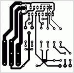
Pls just look pdf for my todays job.
I tried to copy the style of "LM4780 SS Pcb" which appreciated by many members. My layout may be looks like pinkmouse's pcb but may not technically similar or correct.
But, if I remember "That route can never be short !!!!!!!!!!!!" I should concentrate to another layout.
Best Regards.
"YOUR DREAM DOESN'T HAVE AN EXPIRATION DATE. TAKE A DEEP BREATH, AND TRY AGAIN."
Pls just look pdf for my todays job.
Attachments
Must the LM1876 have both pins 2 and 15 connected?
Attachments
Yes I can see you have them both connected.
Must they be? Or can you use just one?
I really do not know this and im curious about it.
Must they be? Or can you use just one?
I really do not know this and im curious about it.
OK,
if there is an alternative to choose from, either pin 2 or pin 15 connected.
Then I believe you have a possibility to make a much smaller PCB and realise Andrews advise in that.
if there is an alternative to choose from, either pin 2 or pin 15 connected.
Then I believe you have a possibility to make a much smaller PCB and realise Andrews advise in that.
Pin 2 is the Vcc connection for one amp, pin 15 is Vcc for the other. If you measure 0.00 ohms between the pins it may not make any difference, but you most likely have to connect both (because it won't be 0.00 ohms).
This is the typical rubbish posted by ill-informed Members.But the 1876 only has one Vcc Pin.
Take your version of pin outs to another Forum.😀
Oh you deleted the post. How unsporting!
Last edited:
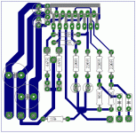
You are on the right track/trace.
Instead of the Zobel coming to the front of the PCB. Could you take it straight back to the decoupling ground?
Ah! single sided stops that. How about a wire link?
RF filters?
Is Pin10 clean? I would take that to Power Ground, if there is a risk it could contaminate Signal Ground.
Instead of the Zobel coming to the front of the PCB. Could you take it straight back to the decoupling ground?
Ah! single sided stops that. How about a wire link?
RF filters?
Is Pin10 clean? I would take that to Power Ground, if there is a risk it could contaminate Signal Ground.
Last edited:
- Status
- Not open for further replies.
- Home
- Amplifiers
- Chip Amps
- LM1876