Hi all,
Recently I've looked through Hitachi amplifiers, their mid-to-high range from '80s, HA-xxxx and HMA-xxxx.
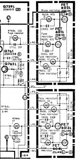
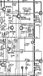
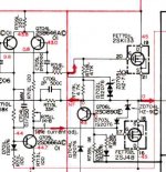
What I found intriguing is that in their "bigger models" they've used small capacitors in parallel gate resistances of output mosfets. The "exceptions" are HMA-6500, where there are no caps across the gate resistors and HA-8700, where on 2SJ49's in only one gate resistance with 1nF parallel cap - for both mosfets. 😕 I've checked also parts list for HA-8700, indeed only one cap is listed on "negative side", for 2SJ49.
I could not figure out the exact reason for doing this way - ok, cap across the resistor can help maybe a bit at high frequencies, but it's not worse from stability point of view ? From what I know reducing gate impedance with raising frequency would not be the best thing to do for a mosfet if you want to avoid oscillations, generally speaking.
Below are some shots from schematics described.
In case of using caps across gate resistors as Hitachi did - how to check for oscillations without a scope (mosfets temperature, zobel burning) ?
Hitachi mosfets are almost unobtainable now - I'm wondering if can we apply this "trick" with the C||R for current production Exicon/Semelab/Alfet/Renesas mosfets (single-die, not dual-die) ?
Any comments and suggestions are welcome.
Thanks,
Tibi
Recently I've looked through Hitachi amplifiers, their mid-to-high range from '80s, HA-xxxx and HMA-xxxx.
What I found intriguing is that in their "bigger models" they've used small capacitors in parallel gate resistances of output mosfets. The "exceptions" are HMA-6500, where there are no caps across the gate resistors and HA-8700, where on 2SJ49's in only one gate resistance with 1nF parallel cap - for both mosfets. 😕 I've checked also parts list for HA-8700, indeed only one cap is listed on "negative side", for 2SJ49.
I could not figure out the exact reason for doing this way - ok, cap across the resistor can help maybe a bit at high frequencies, but it's not worse from stability point of view ? From what I know reducing gate impedance with raising frequency would not be the best thing to do for a mosfet if you want to avoid oscillations, generally speaking.
Below are some shots from schematics described.
In case of using caps across gate resistors as Hitachi did - how to check for oscillations without a scope (mosfets temperature, zobel burning) ?
Hitachi mosfets are almost unobtainable now - I'm wondering if can we apply this "trick" with the C||R for current production Exicon/Semelab/Alfet/Renesas mosfets (single-die, not dual-die) ?
Any comments and suggestions are welcome.
Thanks,
Tibi
Attachments
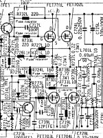

I think that the gate capacitors eliminates stray inductance since the TO-3 power mosfets are not mounted on the PCB but instead wired to the PCB. They may also compensate for the different gate capacitance of the P and N mosfet.
Hope this helps.
Hope this helps.
It's because the P and N channel mosfets have vastly different source to gate capacitances.. It's to try and equal them.
thanks for answers guys
I think that elimination of stray inductance could be the main reason, because for Cgs equalization I've seen caps added on N-ch between G and S...P-ch have anyway a bigger Cgs, I see no reason to add another cap just to increase it further.
Also please note that gate resistors are different values for N-ch and P-ch...this would be the second method in quest for equal "slew rate" between N-ch and P-ch...also mentioned on Exicon app notes.
regards,
Tibi
@MiiB
my guess is no🙂...we have caps in both N-ch & P-ch, usually bigger for P-ch (also bigger Cgs). but there is also an "exception", although cap value doesn't appear in the attach: for HA-7700 both caps are equal, 100pF (C726L & C727L) - indeed, for equal gate resistors
my guess is no🙂...we have caps in both N-ch & P-ch, usually bigger for P-ch (also bigger Cgs). but there is also an "exception", although cap value doesn't appear in the attach: for HA-7700 both caps are equal, 100pF (C726L & C727L) - indeed, for equal gate resistors
my idea is that the 100pF cap helps secure equal drive also at higher frequencies...similar to different gate stoppers at the P and N channel.
well...I've tried adding 33pF for N-ch and 47pF for P-ch...no accoustical change spotted so far.
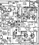
recently I've seen another idea on some Albs schematic....some kind of buffer-resistor between VAS (drivers) and usual gate resistors (attached). R18 and R19 are 8.2 to 10ohm, R20-R25=100ohm. Output FETs are 2SK134/2SJ49, T3-T6 are MJE340/350.
any opinions on this ?
regards,
Tibi
recently I've seen another idea on some Albs schematic....some kind of buffer-resistor between VAS (drivers) and usual gate resistors (attached). R18 and R19 are 8.2 to 10ohm, R20-R25=100ohm. Output FETs are 2SK134/2SJ49, T3-T6 are MJE340/350.
any opinions on this ?
regards,
Tibi
Attachments
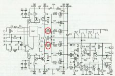
R18 & R19 are to help prevent the Zeners blowing up the driver stage with all it's carefully matched components that took many resources to work well.
Jez has it right. the Hitachi lateral mosfets have huge gate capacitance's and the N and P channels parts are different by quite a bit. the cap is there to try and equalize the differences between the sides. I remember reading an article with a designer that stated exactly that. I think is was Rolf Yeoman from Soundcraftsmen...but it is very early and i am definitely not awake at the moment so i could be wrong about that...
R18 & R19 are to help prevent the Zeners blowing up the driver stage with all it's carefully matched components that took many resources to work well.
but, the additional resistance in the gate feed seriously increases the rise time (slower slew rate) of any signals into the output. i.e. it slew limits HF and transients.I didn't took into account this way 😱 but it's good to have learned it
thank you, AndrewT
Additionally mosFETs perform better when fed from low or very low impedance sources.
Hi, Andrew
Yes, I know that increasing gate resistance we are slowing down the mosfet - but it's maybe somehow good on stability (less prone to oscillations).
I guess it's wiser to keep the "buffer resistors" (like R18 & R19) to a minimum.
I'm thinking at splitting the gate resistor in two parts - let's say 10R + Rvalue-10 - if we have 220R for example than would be 10R "buffer" + 200R "gate". Overall the value (from vas to gate pin of mosfet) will remain the same or at least to be around 90-110% of the initial value.
The only question that remains is if we have more than 1 pair of mosfets - of course it would be like in the Albs schematic posted earlier, but I have some question marks on stability side...worth a try anyway.
Zero Cool - thanks
well...in another thread here I've discovered the same ideea with "buffer" resistors + normal "gate" resistors for the output mosfets - described also in post #8.
this time for sure R16 & R17 are not to prevent Zeners ZD1 & ZD2 to blow the driver stage, because they are connected after the Zeners.
any opinions ? why would be good to split the gate resistor in two ?
regards,
Tibi
this time for sure R16 & R17 are not to prevent Zeners ZD1 & ZD2 to blow the driver stage, because they are connected after the Zeners.
any opinions ? why would be good to split the gate resistor in two ?
regards,
Tibi
Attachments
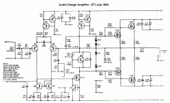
nobody....no ideea on last schematic ?
maybe a link with an JLH/ETI old article referring to/describing this amp ?
regards,
Tibi
maybe a link with an JLH/ETI old article referring to/describing this amp ?
regards,
Tibi
I've found some information about the additional gate resistors here:
"Mods (courtesy of David Huckle) restore additional output gate resistors used in the '84 ETI version that were omitted in the later Hart version. This resolved "a very subtle but different sound... [the] Hart amp definitely did not sound as lucid and fluid... there was a slight hardness or grainy edge to the music right through the scales, on the very best recordings". This might well have represented an oscillation problem."
Link: A Paul Kemble web page - JLH mosfet amplifiers.
Maybe someone has more details about this ?
regards,
Tibi
Attachments
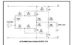
and some information from Randy Slone's book, pages 190-191:
"R1 and R2 provide some additional stabilizing isolation between the relatively high gate capacitance of the lateral Mosfet stage and the VAS."
What is not well known - the value for this "buffer" resistors, I didn't see it discussed/specified anywhere so far. Both Randy Slone and JLH ETI 1984 use 150R, ALBS uses 10R. Would be interesting to find some kind of formula for the right value - or what should be taken into consideration.
As a note - also his OptiMOS design features this kind of "buffer" resistors between VAS and the proper gate-resistors of the mosfets.
Attachments
- Status
- Not open for further replies.
- Home
- Amplifiers
- Solid State
- Lateral mosfet driving question - Hitachi amplifiers