First happy new year to all.
LA4282 datasheet are available both from Sanyo and OnSemi
LA4282 pdf, LA4282 description, LA4282 datasheets, LA4282 view ::: ALLDATASHEET :::
LA4282 pdf, LA4282 description, LA4282 datasheets, LA4282 view ::: ALLDATASHEET :::
At the Digital-Piano DP-263 (McCrypt) of my friend - go to
https://asset.conrad.com/media10/ad...l-304303-piano-mc-crypt-dp-263-dark-brown.pdf
occurs a hard popping while switch-on since any weeks (no OCL circuit, i. e. caps in series to the speakers).
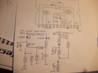
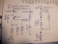
The reason was the shorted diode D1 around the mute control unit and the reason for this was again a bad design of the mute control circuit, because a small signal diode for charging a capacitor with 470uF without a serial resistor isn't a good solution - go to the first attached images and there to the first circuit.
One possibility is the use of a diode like 1N5407 (which I have currently realized as an emergency solution).
Because there are no application notes to this IC it is a bit difficult to find a mute control circuit with a sophisticated design.
After study several service manuals I have found this manual of LG television with chassis MC-014A - go to
LG MC-014A CHASIS Service Manual download, schematics, eeprom, repair info for electronics experts
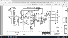
The part of the audio power amp section of the LG chassis MC-014A you will find in the last (third) attachment and the part only for mute control section in the second circuit of first both images.
Here the necessary series resistor was present to limit the charging current for the associated diode. But there are other differences around the base of the transistor.
The MUTE mode in both circuit variants is active, as long as the transistor is in the conducted condition resp. is switched on (while troubleshooting I shorted C-E route of this transistor - therefore I know this exactly).
My questions are follow:
1) What is the task of Dx and the electrolytic capacitor around the base connection of transistor in the first mute control circuit (LG use only a resistor to the positive rail of 9VDC) ?
2) How do I convert the values from the LG-circuit , when I only have 5VDC instead of 9VDC as can be seen in the LG circuit from last attachment (maybe an appropriate modify according to the LG circuit is an approach, which operates better than the introduce of a high-current diode)?
Thank you for replies.
LA4282 datasheet are available both from Sanyo and OnSemi
LA4282 pdf, LA4282 description, LA4282 datasheets, LA4282 view ::: ALLDATASHEET :::
LA4282 pdf, LA4282 description, LA4282 datasheets, LA4282 view ::: ALLDATASHEET :::
At the Digital-Piano DP-263 (McCrypt) of my friend - go to
https://asset.conrad.com/media10/ad...l-304303-piano-mc-crypt-dp-263-dark-brown.pdf
occurs a hard popping while switch-on since any weeks (no OCL circuit, i. e. caps in series to the speakers).
The reason was the shorted diode D1 around the mute control unit and the reason for this was again a bad design of the mute control circuit, because a small signal diode for charging a capacitor with 470uF without a serial resistor isn't a good solution - go to the first attached images and there to the first circuit.
One possibility is the use of a diode like 1N5407 (which I have currently realized as an emergency solution).
Because there are no application notes to this IC it is a bit difficult to find a mute control circuit with a sophisticated design.
After study several service manuals I have found this manual of LG television with chassis MC-014A - go to
LG MC-014A CHASIS Service Manual download, schematics, eeprom, repair info for electronics experts
The part of the audio power amp section of the LG chassis MC-014A you will find in the last (third) attachment and the part only for mute control section in the second circuit of first both images.
Here the necessary series resistor was present to limit the charging current for the associated diode. But there are other differences around the base of the transistor.
The MUTE mode in both circuit variants is active, as long as the transistor is in the conducted condition resp. is switched on (while troubleshooting I shorted C-E route of this transistor - therefore I know this exactly).
My questions are follow:
1) What is the task of Dx and the electrolytic capacitor around the base connection of transistor in the first mute control circuit (LG use only a resistor to the positive rail of 9VDC) ?
2) How do I convert the values from the LG-circuit , when I only have 5VDC instead of 9VDC as can be seen in the LG circuit from last attachment (maybe an appropriate modify according to the LG circuit is an approach, which operates better than the introduce of a high-current diode)?
Thank you for replies.
Attachments
Last edited:
The cap on the base of the transistor looks like a time delay. It'll keep the PNP on for a while after power-up, which will activate the mute. The purpose of the path through DX is to discharge the cap on power-down. The 470 uF on the emitter is likely there to prevent the PNP from oscillating.
I don't see how the second circuit can create a brief mute on start-up, which I assume is the purpose of the circuit.
The diode on the output of the circuit is half of an "OR gate", by the way. The mute signal is high when the signal from S-MUTE is high OR the signal from the PNP is high.
If your goal is to repair the first circuit, why not simply insert 47 Ω in series with the 1N4148 on the emitter of the PNP and be done? That would limit the charging current through the diode to about 100 mA. I seem to recall that an 1N4148 can handle 2-3 times that. I'm curious why that diode is there in the first place. I suppose it could be to protect against reverse biasing the B-E junction in the PNP on power-down.
Tom
Last edited: