I'm planning on putting together a board i bought a long time ago from the Orient, via eBay. It's a JLHC, but I don't have too much more info than that. I also have 8 "Arctic 12 Passive" heatsinks that I thought I could use with this. (They are "rated" at 47W each!?) I can't find out too much information about this particular board and wonder if anyone here has built one of these 4 OP transistor amps. I think it was rated at 15w when I bought it.
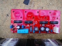
I had planned to separate the transistors onto their own heatsinks, as they seem a bit close to each other on the board. Is this wise? I wonder if that's why the vendor recommended a 15-0-15 200VA supply (I presume per side?). Could the output increase with a larger supply and sufficient space and sinking? Is there any existing guide for setting such an amp up?
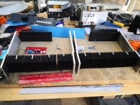
Is a regulated supply the way to go with this board? I've seen a JLH update page with a diagram for a regulated supply, but wonder if it's sufficient for this board with it's increased output devices. I presume I'd have to get an 18-0-18 supply to get a 15-0-15 regulated output? (That's what the rear heatsinks could be for.)
Or would it be a better idea to go for a different design to fit my proposed case hardware (because I have it lying about)? I'm thinking for a mirrored dual mono design that I can sit next to each other, with the fins out the sides. I'd like to squeeze as much power out of these heatsinks as I can!
I welcome any suggestions, knowledge, encouragement, intrigue, or slight criticism.
P.S. At the bottom of one of the images is another set of thin boards. I have no idea what they are are, aside from being cloned Class A amp boards, using a 7 leg 2SJ109, a ZTX450 and ZTX550, with 4 IRFP240 output drivers. Any info on these mystery boards would be publicly thanked.

I had planned to separate the transistors onto their own heatsinks, as they seem a bit close to each other on the board. Is this wise? I wonder if that's why the vendor recommended a 15-0-15 200VA supply (I presume per side?). Could the output increase with a larger supply and sufficient space and sinking? Is there any existing guide for setting such an amp up?

Is a regulated supply the way to go with this board? I've seen a JLH update page with a diagram for a regulated supply, but wonder if it's sufficient for this board with it's increased output devices. I presume I'd have to get an 18-0-18 supply to get a 15-0-15 regulated output? (That's what the rear heatsinks could be for.)
Or would it be a better idea to go for a different design to fit my proposed case hardware (because I have it lying about)? I'm thinking for a mirrored dual mono design that I can sit next to each other, with the fins out the sides. I'd like to squeeze as much power out of these heatsinks as I can!
I welcome any suggestions, knowledge, encouragement, intrigue, or slight criticism.
P.S. At the bottom of one of the images is another set of thin boards. I have no idea what they are are, aside from being cloned Class A amp boards, using a 7 leg 2SJ109, a ZTX450 and ZTX550, with 4 IRFP240 output drivers. Any info on these mystery boards would be publicly thanked.
Separating MOSFETs into independent heatsinks seems to me to be useless. Runing all them toguether cooperates to current sharing too. If one of them tend to run hotter, their internal resistance increases, forcing the others to take its desired current. Finally an equilibrium will establish.
The heatsinks won't be independent. I can create isolated TO3 mounting fixtures, but the heatsinks will all be bolted together, as part of the chassis.
The coupling of heatsinks for thermal equilibrium needs to be very tight indeed if that is a requirement of the amplifier design, such as a class AB type. Thermal conduction is very slow in comparison to the rapidly changing heat produced within the power transistors, whatever the class of operation, so one heatsink with a thick backplate, is a somewhat better plan than a number of small heatsinks coupled only by sheet metal or other small cross-section forms.
However, the function of either power transistor in the JLH class A design is not the same balanced type as in push-pull class A, AB, B etc. One transistor is effectively a bias controller for the other here. If possible, read JLH's original description and design notes here: www.keith-snook.info/wireless-world-magazine/Wireless-World-1969/Simple%20Class%20A%20Amplifier%20-%20.pdf
Accordingly, bias just has to be enough to maintain class A operation and in principle, it doesn't matter if the 2 power transistors are coupled or not, though there may be wider differences between either stereo channel when compromised by the power supply or different construction, for example.
Thanks for the comment. You say thermal conduction is slow in comparison to heat produced, whatever the class of operation, but you later say that coupling is not important in a class A design with 2 power transistors. The design I have has 4 of them though. I did imagine the heatsinks will all be firmly polished and bolted together and to the chassis. I will be using at least 10mm plate (depicted) for this, since I do have some basic machining facilities. Thanks for linking the article. I have a copy of JLH's book on class A amps that was published consequently, but neither of them have quite this exact design published in them.The coupling of heatsinks for thermal equilibrium needs to be very tight indeed if that is a requirement of the amplifier design, such as a class AB type. Thermal conduction is very slow in comparison to the rapidly changing heat produced within the power transistors, whatever the class of operation, so one heatsink with a thick backplate, is a somewhat better plan than a number of small heatsinks coupled only by sheet metal or other small cross-section forms.
However, the function of either power transistor in the JLH class A design is not the same balanced type as in push-pull class A, AB, B etc. One transistor is effectively a bias controller for the other here. If possible, read JLH's original description and design notes here: www.keith-snook.info/wireless-world-magazine/Wireless-World-1969/Simple%20Class%20A%20Amplifier%20-%20.pdf
Accordingly, bias just has to be enough to maintain class A operation and in principle, it doesn't matter if the 2 power transistors are coupled or not, though there may be wider differences between either stereo channel when compromised by the power supply or different construction, for example.
Are you saying that it it simply not worth using multiple heatsinks for the losses during heat transfer and inability to reach thermal equilibrium? With my first two thread responses focusing on this one aspect, it does seem particularly important, although I can't see why: Since the interface between each transistor and heatsink already has this inefficiency over less surface area.
I see the designation MJ21194 🙂IRFP240 output drivers
This is a 2003 modification. Lots on the internet and on this site.Not installed on PCB 2SC3421 , 2SA1358.
Two separate power supplies are usually used for power. Each has a bipolar voltage -15v-0-+15v.
It is possible to use MOSFET at the output. For example SK1529\1530.
Freestanding heatsinks are preferred, but they must be electrically isolated from the chassis and from each other. Avoid electric shock!
Last edited:
Thanks and apologies for the confusion: There are 2 different sets of boards in the pictures. I don't think the long, thin IRFP240 boards mentioned are JLH ones, cince they have these 2SJ109 differential amp 7 pin modules and are long and thin to provide thermal spacing to bolt the 4 x TO-247-3 style output transistors directly to a flat heatsink. The MJ21194 output devices are for the "updated" JLHC boards though.I see the designation MJ21194 🙂
This is a 2003 modification. Lots on the internet and on this site.
I was thinking about how big this amplifier will be. If i stick to a low power design, then it might be better if the amp format was stereo. I've been using 10mm plate for various projects, sourced from some bloke making big holes and then selling 325mm laser cut, 10mm thick disks on eBay. I discovered last night that a 10 sided polygon with sides of 10cm (the size of each heatsink) will come to just a bit less than 325mm for it's major diameter. It's too much of a coincidence, perhaps! This means I could use such disks to be the top and bottom plates for a circular amp design that has 4 heatsinks per side and relatively tiny front and rear 10cm panels.
Not the most practical of shapes, I admit.
Risk of electric shock if transistors are not isolated from heatsinks. Risk of burns - class A amplifier can be hotter than 50"CNot the most practical of shapes, I admit.
But we hardly even know each other!2SK1529\1530
Can you say what that has to do with shape? I'd have thought the extra space around each heatsink would make it more thermally efficient than having them right next to each other.Risk of electric shock if transistors are not isolated from heatsinks. Risk of burns - class A amplifier can be hotter than 50"C
I didn't see you'd edited your previous post with additional information - thank you. I have some D669AC and B649AC devices that were supplied, but I haven't got round to finding out which one goes where yet, or if they are correct equivalents. I also assume these don't need any heat sinking...2SK1529\1530
The proposed design includes isolation between output transistors and heatsink (they provided an angle plate) via TO3 mica washers and mechanical connection with bolts (isolated from the heatsink) carrying the signal to the transistor's can. I feel this amount of heatsink is too large an area to electrically isolate from a chassis, while maintaining adequate ventilation and safety against accidental external shorts.
Thanks. It was just a whim, based on the materials I have available. I was thinking I could machine 10 thick posts with 144 degree faces that bolt-join each heatsink to it's neighbour, while also having threaded holes top and bottom to secure the plates with circles of bolts. It might end up looking like an attack-Roomba. It will be ridiculously solid, but perhaps it is a bit too silly and hard to move (unless I add wheels, of course....)I think it's a really neat shape for an amp. Reminiscent of a Cray supercomputer.
But I'd not want to pick up any amp by it's heatsinks unless a lot of care had been taken to secure them. Mechanically it's likely to be a weak point. Rack handle(s) across the top?
I could always add something protective to fill the gaps between the heatsinks, like 8 grab handles integrated into these machined posts I'm trying to visualise. They would stick out to protect the extremities of the fins. I wonder if that's possible. I am into metalworking, but I have to be careful not to "go ham". For example, in one of my pictures (on top of my bench power supply) there is a case I made for a tiny 1W amp that I'd admit is slightly "over-engineered". I'm also on a roll from recently re-imagining my preamp, but with floating, back-lit, soft-touch buttons:
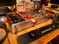
If the 1996 JLHC design needs a regulated supply then I'm not sure this crazy case will be big enough for the extra regulators and maybe it might be better to use an alternative design, like Doug Self's unregulated "Trimodal" one to be a better fit in this configuration of case, or a more sensible dual-mono rectangle with additional heatsinks for a regulated JLH approach.
Last edited:
Let us be careful here. What I referred to was that the "output transistors" are not a simple complementary pair, such as you find in common class B or AB amplifiers. In JLH's design, TR2 has the independent function of a dynamic load for TR1, the output transistor here. See figures 1,2,3 and the text in the introduction of the original magazine article linked in my post.......but you later say that coupling is not important in a class A design with 2 power transistors....
Last edited:
It reminds me of a simulation of an amp schematics .
(original form, works well in simulation, but super boring to implement and realize and in the end only brings inconveniences in real life)
Assemble a pair of amps on the table and listen to them for a few days before embarking on such a project because the purpose is always listening and if you are disappointed, it will cause you disappointment for a while.
That's great advice - I wish someone had told me that before I built my transmission lines!It reminds me of a simulation of an amp schematics .
(original form, works well in simulation, but super boring to implement and realize and in the end only brings inconveniences in real life)
Assemble a pair of amps on the table and listen to them for a few days before embarking on such a project because the purpose is always listening and if you are disappointed, it will cause you disappointment for a while.
Really sorry, but I don't understand the relevance of this. Would having different thermal dissipation rates on JLH Class A output transistors affect the heatsinking design? It does not appear that way on this particular PCB, since the 4 output device positions are right next to each other. I did suggest I should separate them in my original post... I don't know about the being careful, but you did say "accordingly, bias just has to be enough to maintain class A operation and in principle, it doesn't matter if the 2 power transistors are coupled or not". I have read the PDF you supplied, and the JLH book, and am still none the wiser over what you're trying to tell me, unfortunately.Let us be careful here. What I referred to was that the "output transistors" are not a simple complementary pair, such as you find in common class B or AB amplifiers. In JLH's design, TR2 has the independent function of a dynamic load for TR1, the output transistor here. See figures 1,2,3 and the text in the introduction of the original magazine article linked in my post.
in fact, on the jlh69 design (if this is the one we are talking about) only one of the two output transistors "sees" the signal, the other serves as a current amplifier but does not "see" the signal.
Ian directed you to the original article by Mr Hood which clearly explains the importance of work on the "active" components and mainly on the final transistors, there is even a table giving the rate of distortion according to the choice of gain of the power transistors and even depending on whether they are balanced or not.
Mr Hood's original schematic is like fried eggs, extremely simple to make, hard to miss, but extremely hard to turn it into something extraordinary, but when you get there (with work and time) it's is one of the best "daily" that I have known so far, it does not do everything well, but what it does is a real pleasure on a daily basis.
- Home
- Amplifiers
- Solid State
- JLH Class A design issues - that sinking feeling