I'm trying to help a friend repair a M600/1 amp.
Initially, the amp wouldn't stay powered on. My friend replaced the 6 FETs that are part of the power supply. They blew immediately when it was plugged back in.
Next, the 4 output FETs were replaced along with the six power supply FETs. This time, we were investigating in my workshop so we had a little bit better tools available.
With all 10 FETs replaced, we tried powering the "main board" up with the preamp board unplugged.
The amp would draw about 63mA with the remote unpowered and no load connected.
As soon as the remote was given 12V, the power supply that I had it on hit current limit at 10A and within a second, the 4th FET from the edge of the circuit board was fried, using a FLIR camera to identify it.
We desoldered and replaced the FET and tried again, this time with a power supply that would feed 30A. The results were nearly identical - within half a second or so, the fifth FET from the edge in the power supply popped.
I replaced it, signed up for this forum and waited to be able to post.
I'm looking for a little direction. I have all the tools - scopes, FLIR, signal generators, power supplies, solder, desolder, microscopes. I don't have familiarity with ClassD amp troubleshooting.
I found:
and a few others.
I'm wondering about a strategy for troubleshooting this. Things that I've seen recommended:
-Removing the 4 output FETs altogether, try to test output of power supply
-Removing the 4 output FETs, jumping (I assume) Drain and Source, looking for square wave on output from power supply
-Removing all 6 FETs on the power supply, checking G-S drive voltage on all 6
I am pretty sure that my power supply is driving into a short, somewhere, based on the inrush current when the thing is trying to start and the PS FETs blowing up real fast. Don't really know where to go from here. Any thoughts on strategy or pointers on things to read appreciated.
TIA
-Dave
Initially, the amp wouldn't stay powered on. My friend replaced the 6 FETs that are part of the power supply. They blew immediately when it was plugged back in.
Next, the 4 output FETs were replaced along with the six power supply FETs. This time, we were investigating in my workshop so we had a little bit better tools available.
With all 10 FETs replaced, we tried powering the "main board" up with the preamp board unplugged.
The amp would draw about 63mA with the remote unpowered and no load connected.
As soon as the remote was given 12V, the power supply that I had it on hit current limit at 10A and within a second, the 4th FET from the edge of the circuit board was fried, using a FLIR camera to identify it.
We desoldered and replaced the FET and tried again, this time with a power supply that would feed 30A. The results were nearly identical - within half a second or so, the fifth FET from the edge in the power supply popped.
I replaced it, signed up for this forum and waited to be able to post.
I'm looking for a little direction. I have all the tools - scopes, FLIR, signal generators, power supplies, solder, desolder, microscopes. I don't have familiarity with ClassD amp troubleshooting.
I found:
Hey everyone, got a JL Audio 500/1 that i disassembled to paint the heatsinks, unfortunately when reassembling i forgot to put insulator between output mosfets and the heatsink. when powering up i got green light, then low load warning light and smoke, i quickly disconnected power supply. upon first inspection i got one of output fets fried and 5 power supply transistors shorted. power supply gate resistors all measure about 47 ohm. any chance i can fix the thing just just using my soldering skills and a multimeter? i dont have oscilloscope on hand, any help would be appreciated.
Best regards
Best regards
- moochinazz
- Replies: 60
- Forum: Car Audio
I'm wondering about a strategy for troubleshooting this. Things that I've seen recommended:
-Removing the 4 output FETs altogether, try to test output of power supply
-Removing the 4 output FETs, jumping (I assume) Drain and Source, looking for square wave on output from power supply
-Removing all 6 FETs on the power supply, checking G-S drive voltage on all 6
I am pretty sure that my power supply is driving into a short, somewhere, based on the inrush current when the thing is trying to start and the PS FETs blowing up real fast. Don't really know where to go from here. Any thoughts on strategy or pointers on things to read appreciated.
TIA
-Dave
Photo of the board in this amp?
What are they using for the drive circuit in the output stage?
Did you test the drive circuit with a load prior to installing the PS FETs?
What are they using for the drive circuit in the output stage?
Did you test the drive circuit with a load prior to installing the PS FETs?
Photo: tomorrow or Friday, when I next have time to get down there. Typical JL construction: 6 FETs on right side with inductors for power stage, 4 FETs on left for output. Could be a spitting image of other single channel JL amps pictured here.
Drive circuit: not sure. Any thing to read to learn how to figure it out? Are you talking about like what kind of FET drivers they're using?
Drive circuit test: no, didn't test with a load prior to reinstalling PS FETs. Replaced all 4 drive FETs, didn't test drive circuit.
Of note: two surface mount resistors close to the 4 drive FETs were noticeably hotter than the rest of the circuitry in the area. 0805 size maybe?
TIA. I'm going to try to get the flash compatible browsers set up, Perry. Your tutorial sounds like a bargain, would love to get set up with it. I much prefer reading material to handholding. If nothing else, I'd like to support you because you've been piping up on countless threads and I've learned a lot reading your posts already.
If you get the Flash capable browsers installed, you're doing better than most. When I mention that people cannot use their preferred browsers,... end of conversation. The site below has all you need to get the files installed.
https://www.bcae1.com/temp/!_READ-ME_if_you_want_to_view_the_Flash_files.htm
You will have months of reading if you read most all of it. I've been working to replace many of the oldest, worst quality graphics. They're mostly on pages that will never be read but it's been something that's been bugging me.
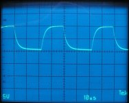
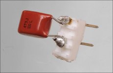
You should always check the drive circuit with a load. I use a 0.047uf cap (seen below). A 0.1uf to a 0.01uf works well for the power supply. The header is to make it more robust and easier to handle. The last image is what to expect with 47 ohm gate resistors and the loading caps mentioned.
The waveform without a load, even with a defective driver circuit, may look like a clean square wave but when loaded, it can' pull back to ground. The scope image below is what a loaded circuit will look like for a good drive circuit. If it's not good, the waveform won't go back to ground as is shown.
Let me know if you have any other questions.
https://www.bcae1.com/temp/!_READ-ME_if_you_want_to_view_the_Flash_files.htm
You will have months of reading if you read most all of it. I've been working to replace many of the oldest, worst quality graphics. They're mostly on pages that will never be read but it's been something that's been bugging me.
You should always check the drive circuit with a load. I use a 0.047uf cap (seen below). A 0.1uf to a 0.01uf works well for the power supply. The header is to make it more robust and easier to handle. The last image is what to expect with 47 ohm gate resistors and the loading caps mentioned.
The waveform without a load, even with a defective driver circuit, may look like a clean square wave but when loaded, it can' pull back to ground. The scope image below is what a loaded circuit will look like for a good drive circuit. If it's not good, the waveform won't go back to ground as is shown.
Let me know if you have any other questions.
Attachments
FYI, this was much easier than your methods for enabling flash:
https://ruffle.rs/#releases
I spent about 20 minutes chasing versions of things. I then got frustrated, did a little googling and had it working in under a minute using current version of firefox that I was already using.
I'll get back to the amp tomorrow.
https://ruffle.rs/#releases
I spent about 20 minutes chasing versions of things. I then got frustrated, did a little googling and had it working in under a minute using current version of firefox that I was already using.
I'll get back to the amp tomorrow.
Ruffle doesn't work offline.
Did you follow the link I posted? All files you need are there. You can have everything installed in less than 5 minutes.
Did you follow the link I posted? All files you need are there. You can have everything installed in less than 5 minutes.
Ok... Pictures.
https://photos.app.goo.gl/hmbitetugAx1axap9
You can see the 5th FET from the left has been removed ... because it blew.
https://photos.app.goo.gl/hmbitetugAx1axap9
You can see the 5th FET from the left has been removed ... because it blew.
Did you check the drive circuit yet?
If you remove the PS FETs (to check the drive), check to see if any of the op-amps have supply voltage without them being in the circuit.
In the future, please post the images to the forum instead of an outside server. We've lost too many images in posts where the poster removed them or lost the account they're posted to. Posting to the forum server will ensure that they will always be available.
- Home
- General Interest
- Car Audio
- JL M600/1 repair