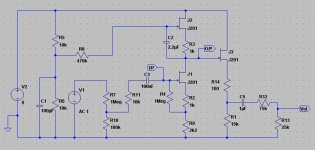
Hi guys. I'm simulating the following SRPP stage in LTSpice:

The idea is to use it as a clean boost stage so driving it into clipping is not the aim. It must accept a range of input signals up to about 1V which explains the additional R9. I added this to lift the DC levels of J1 and, I would think, offer greater headroom at the input. Yes it cuts down on headroom at its drain but that I can spare. For bigger signals I can switch the rail voltage to a generated 16.5V and more than regain it. Thankfully all that seems to be what I'm seeing.
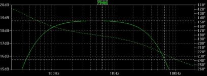
Originally I set it up without R7 and R10 in place with the input from V1 connected directly to R11. The frequency response top end was flat to way beyond the audio range. I didn't think there was anything odd in adding a divider (simulated drive control) to the input which may have allowed me to remove R9 but when I did I got the following response plot:

The top end rolloff now displays a 3dB point of 6.6kHz. Investigating a little further shows that any series resistance in that input line, adding a series parasitic resistance to V1 for example, affects the upper rolloff.
Now I can't really see any mechanism which would account for this but then I'm much more a BJT than a JFET man. Maybe the additional R9 in the source line is having an effect I did not anticipate. Can anyone explain what I am seeing here?
The idea is to use it as a clean boost stage so driving it into clipping is not the aim. It must accept a range of input signals up to about 1V which explains the additional R9. I added this to lift the DC levels of J1 and, I would think, offer greater headroom at the input. Yes it cuts down on headroom at its drain but that I can spare. For bigger signals I can switch the rail voltage to a generated 16.5V and more than regain it. Thankfully all that seems to be what I'm seeing.
Originally I set it up without R7 and R10 in place with the input from V1 connected directly to R11. The frequency response top end was flat to way beyond the audio range. I didn't think there was anything odd in adding a divider (simulated drive control) to the input which may have allowed me to remove R9 but when I did I got the following response plot:
The top end rolloff now displays a 3dB point of 6.6kHz. Investigating a little further shows that any series resistance in that input line, adding a series parasitic resistance to V1 for example, affects the upper rolloff.
Now I can't really see any mechanism which would account for this but then I'm much more a BJT than a JFET man. Maybe the additional R9 in the source line is having an effect I did not anticipate. Can anyone explain what I am seeing here?
Attachments
I can't see any SRPP in that circuit, just an active load.
Your HF rolloff is probably due to Miller effect. You have changed your source impedance from 10k to 100k (roughly). This will drop the HF corner frequency by a factor of 10.
This is not a BJT or FET issue - it happens with any inverting amplifier with capacitance between input and output.
Your HF rolloff is probably due to Miller effect. You have changed your source impedance from 10k to 100k (roughly). This will drop the HF corner frequency by a factor of 10.
This is not a BJT or FET issue - it happens with any inverting amplifier with capacitance between input and output.
As a side note, I don't much see the point here.
You specify "clean boost" and "1 V input".
The circuit you posted has very high gain, but in practice a 9V battery can give you no more than 3V RMS (and that with difficulty), so max allowable gain would be 3X ... your circuit provides way above that.
Doubling supply voltage would allow twice as much, still not enough for 1V input.
I guess a simple 1 Fet stage would be more than enough, and far more adequate (within your constraints).
The SRPP side of it is covered here. It may not be fully applicable but as I understand the circuit action, (not immediately obvious), it can be described as SRPP. It's really a step beyond the most common name given to it, the mu-amp which is not strictly correct.
http://www.geofex.com/Article_Folders/modmuamp/modmuamp.htm
Of course I do understand that there are shared characteristics between FETs and BJTs, my comment was only to show I'm aware of the fact that it may just be something which FETs are prone to that BJTs are not, e.g. I'm not too up on the scale of parasitic capacitances for FETs whereas I'm familiar with them for BJTs.
At first when I read your reply I thought "It can't be plain Miller effect, it must be way too big?" But with 100k(ish) source impedance and a corner frequency of 6.6kHz we are looking at a capacitance of about 0.24nF. The gain is roughly 20dB so the Cgd (?) would be in the region of 24pF wouldn't it? That seems a bit high but it is getting to the range I would have expected for Miller capacitance.
I've just thrown a cascode BJT into the sim between the 2 JFETs, (I wouldn't expect it to work as a serious solution but it should serve to decrease the Miller effect), and you are right, it does straighten out the top end. (Mind you the bottom end is a rising mess now and the gain has dropped some 16dB, but your point is well made. 😀 )
So how do so many effects pedals get away with slinging 1M potentiometers on the front end before their JFET gain stage? They sometimes have a bypass cap between the wiper and the hot end but simulations show that's a fudge. Yuk! It could suggest the need for maybe a low output impedance buffer at the front.
Many thanks for pointing me to what should have been the blindingly obvious but which I needed a slap to see. I'm a little wiser!
I wouldn't take too much notice of that page. For a start the author doesn't understand how to reduce thermal noise, so his suggested bias 'trick' does nothing. Your C1 bypasses PSU ripple and noise, but does virtually nothing for thermal noise which fortunately is not a problem here anyway. It is C2 which gets rid of thermal noise from the bias network. His explanation of the so-called 'JFET mu amp' is wrong; it is just a (poor) active load circuit. His final circuit is an SRPP but I suspect he doesn't really know how it works.Albertb said:The SRPP side of it is covered here. It may not be fully applicable but as I understand the circuit action, (not immediately obvious), it can be described as SRPP. It's really a step beyond the most common name given to it, the mu-amp which is not strictly correct.
http://www.geofex.com/Article_Folder...p/modmuamp.htm
Your circuit is not an SRPP. An SRPP takes its output from the top of your R3, not the bottom. However, as it is followed by a source follower it doesn't make much difference, as you don't need the reduced output impedance a real SRPP gives. Best to get the name right, though.
A 1M pot has a maximum output impedance of 250k so it could lead to some HF rolloff, but then many guitar amps roll off quite early anyway.
Dooohhhh! Another Homer moment.
You're absolutely right! I have just noticed thanks to your post that I have the schematic laid out wrongly around J2. I should of course have taken the output from the top of R3 as you have said.
Damn it! That was one of the reasons I started to play with this circuit in the first place, I was trying to improve on other mu-amp designs which made exactly the same mistake by doing it "properly" and I missed the most important change in my drafting. And I spent some time gaining a bit of understanding of it too! That was just a stupid slip and makes all of your comments clear.
I understand what you are saying about the following follower as it were. Though with the takeoff in the right place maybe I can get away without it now. It might pay to just leave it in, unknown cable capacitance is always an issue for a guitar application and it never hurts to have a lower output impedance.
So you answered my original question and put right a glaring error on top. That's real value for money in my book. Many thanks for your time, it's been a pleasure being corrected by you DF. 😀
Hi JM, I almost missed your reply in the action with DF. My apologies.
Yes, you are absolutely right with your comments about signal levels and headroom but in this type of application I have a requirement to be able to cope with a wide variation of input devices, (i.e. guitars). Guitar outputs are ridiculously variable. Some will give only a few 10s of mVs and others almost 1V. It's important to have enough gain for the smallest and a way of coping with the largest.
Hence the need to get more gain than really required out of it but to get the input drive attenuation to work without changing the frequency response. I figured if I understood how to maximise the circuit gain I could always reduce it down to whatever was optimal afterwards.
Although I have plans to add a simple overload indicator to show when I approach clipping it is always possible to set up a Boost by ear. With it off you hear your maximum clean level, with it on you just up it as required making sure that's not to the point of being able to hear a distinct change in character. Belt and braces usually does the job. Usually a pedal of this sort would be preceded by a higher gain overdrive/distortion type, with a level control at its output of course. That way you can set the character of sound you want and use the boost to just lift it for certain passages without changing it's quality.
This topology has the advantage over a single FET stage that it is self-centreing. I always think it is really a half job to design a circuit where you have to trim it for its quiescent point depending on device parameters. A circuit should just work with any device (within reason of course). As we know, JFETs are ridiculously variable in terms of gain but if we can get things to be reliably repeatable it is a real step forward.
Last edited:
- Status
- Not open for further replies.
- Home
- Amplifiers
- Solid State
- JFET SRPP circuit frequency oddity