Greetings from Italy!
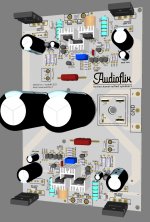
I've decided to make a PCB based on the JAT501 project, I did a bunch of tests on a prototype PCB (mono) and the results are stunning, so I've designed a final PCB which incudes two mono stages and the power supply rectifying stage.
I think I would take the BD139 (voltage amplification) out of the PCB and and screw it to the heatsink, so it can be termal coupled with the 2SC5200 and the 2SA1943. Do you guys think it's a good idea? Instead of using a single heatsink like the ones used on the drivers stage (BD139-BD140)...
Here is the PCB:
Attachments
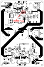
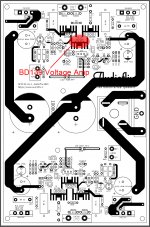
According to the schematic I found, the BD139 is not the VAS transistor but in fact the bias spreader. That is a poor design from a thermal perspective; ideally both the bias spreader and the driver transistors should be on the heatsink with the outputs, so you were on the right path there.
I can't really tell what you supply routing is like; since the usual goal is keeping V+ to V- and V+/- to GND return parasitic inductance low, you tend to end up with elongated layouts spread alongside the heatsink with V+ and V- routed right next to each other.
I can't really tell what you supply routing is like; since the usual goal is keeping V+ to V- and V+/- to GND return parasitic inductance low, you tend to end up with elongated layouts spread alongside the heatsink with V+ and V- routed right next to each other.
I've already made a better version 😉Hi,
John did update the final changes of the design, you can watch his video for details.
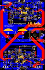
Stereo single layer:

Can you please share your layout for black and white toner transfer diy homemade pcb
Can you post the schematic of your version and the gerber files to have your design made. Great work.
Attachments
Nice work. Johns name or mention on PCB would be in appreciation of his work as he has shared lots of informative videos on you tube.
Best regards
Best regards
@Ciro82 ciao Ciro, I was looking for this board in the past having followed JAT videos since 2018.
I’m living in Italy, would be possible to buy from you some kiy or even the assembled version?
If so it would be great. I have really limited time today to build an amplifiers but I’m still really curious to listen to the JAT 501.
Pls let me know. Image my surprise when I come up after years to your post…
Have a nice end of 2024
My Best
Lorenzo
- Home
- Amplifiers
- Solid State
- JAT501 (John Audio Tech) replica