Amateur level status person here...
Just picked up a non-working Luxman LX-104 stuck in protection.
Have verified that it will come out of protection if I disconnect R channel from protection board.
Found negative rail voltage floating on output of R channel (present on Base and Emitter of all outputs of R, but not L channel).
Pulled R channel outputs and tested on a cheap and cheerful small ebay component tester. All seem to test fine.
No fuses blown and current draw at rail fuses is nominal.
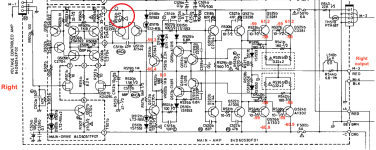
Have done an in-circuit test of all other small signal transistors and have found no shorts. But, I can't really access the ones on the "Main Drive" daughter boards as seen in the attached schematic.
So I thought, if it's possible, that I would like to power it up (even at 1/4 or 1/2 power via Variac) with the outputs removed to run some left to right channel voltage comparisons to see if I could identify where the errant voltage is coming from?
There is I assume also the possibility that the outputs are faulty and just not showing the fault at low voltage? And if this is the case I should see no voltage at the B and E pads with the outputs removed?
So, can someone tell me if the amp can be powered up sans outputs?
Or so I need to solder in some temp components to make it stable?
Thanks in advance.
PS, the numbers in red are the voltages I took when I realized what was going on.
Q514 is a 2sc1845 also attached to the heatsink near the outputs.

Just picked up a non-working Luxman LX-104 stuck in protection.
Have verified that it will come out of protection if I disconnect R channel from protection board.
Found negative rail voltage floating on output of R channel (present on Base and Emitter of all outputs of R, but not L channel).
Pulled R channel outputs and tested on a cheap and cheerful small ebay component tester. All seem to test fine.
No fuses blown and current draw at rail fuses is nominal.
Have done an in-circuit test of all other small signal transistors and have found no shorts. But, I can't really access the ones on the "Main Drive" daughter boards as seen in the attached schematic.
So I thought, if it's possible, that I would like to power it up (even at 1/4 or 1/2 power via Variac) with the outputs removed to run some left to right channel voltage comparisons to see if I could identify where the errant voltage is coming from?
There is I assume also the possibility that the outputs are faulty and just not showing the fault at low voltage? And if this is the case I should see no voltage at the B and E pads with the outputs removed?
So, can someone tell me if the amp can be powered up sans outputs?
Or so I need to solder in some temp components to make it stable?
Thanks in advance.
PS, the numbers in red are the voltages I took when I realized what was going on.
Q514 is a 2sc1845 also attached to the heatsink near the outputs.
Split R532a in 2x 120ohm in series and use the midpoint as connection for the negative feedback. Than I expect no issues, even at full rail voltages.
I think you've got your Base and Emitter voltages mixed up on the 'good' channel.
Almost certainly there'll be +/-0.6v on the Bases and 0.v on the Emitters.
Yes it'll be safe to run without the O/P Transistors.
Sometimes a diode to mimick the Base/Emitter junction can be useful I find.
P
Almost certainly there'll be +/-0.6v on the Bases and 0.v on the Emitters.
Yes it'll be safe to run without the O/P Transistors.
Sometimes a diode to mimick the Base/Emitter junction can be useful I find.
P

Thank you, that is very helpful.
I will give it a shot. But first it just occurred to me that maybe it would be useful to temporarily re-install the outputs and fire it up (maybe at reduced voltage) and take measurements at the 1-7 connection points to the daughter board. If Q507 failed and I get rail voltage at pins 4 and 6 then the FET 2Sk240 (Q501) could have failed open? I don't think I found a short there, but will double check.
I will give it a shot. But first it just occurred to me that maybe it would be useful to temporarily re-install the outputs and fire it up (maybe at reduced voltage) and take measurements at the 1-7 connection points to the daughter board. If Q507 failed and I get rail voltage at pins 4 and 6 then the FET 2Sk240 (Q501) could have failed open? I don't think I found a short there, but will double check.
I concur that the circuit can safely operate without the output devices, but I suspect the problem may may be in the early stages and suggest some voltage measurements, using the working channel for reference.
Note that collector of Q511b is at -59.3V. If feedback were operating properly, Q511b would conduct to raise collector voltage to just above 0V but that’s not happening. Given that amp output is stuck near the negative rail, I project the following should be observed:
Feedback voltage to gate of Q501b will be several volts more negative than the gate of the input FET(~0V). Consequently, Q501b and Q506b should be off, and the input FET and Q505b should conduct. Q512b and Q511b should conduct in response and raise the output.
But I imagine that the circuit will fail to follow this description and hope that the discrepancy will reveal the culprit.
Good luck!
If no fuses blown and no sign of transistors shorted and found negative rail voltage floating on output, in most cases is caused by opened resistorsFound negative rail voltage floating on output of R channel (present on Base and Emitter of all outputs of R, but not L channel).
Pulled R channel outputs and tested on a cheap and cheerful small ebay component tester. All seem to test fine.
No fuses blown and current draw at rail fuses is nominal.
Have done an in-circuit test of all other small signal transistors and have found no shorts. But, I can't really access the ones on the "Main Drive" daughter boards as seen in the attached schematic.
please check the resistor R516b in the R channel
Attachments
I think you've got your Base and Emitter voltages mixed up on the 'good' channel.
Almost certainly there'll be +/-0.6v on the Bases and 0.v on the Emitters.
Yes it'll be safe to run without the O/P Transistors.
Sometimes a diode to mimick the Base/Emitter junction can be useful I find.
P
Yes, you're correct. I just double checked and I did flip those measurements. Still developing my skills. Thanks.
I tacked back in the outputs for the right channel and took the measurements at the connection points 1-7 for the daughter boards.
Right channel:
1 = 60.4
2 = 59.3
3 = 59.8
4 = 59.8
5 = 59.3
6 = 59.8
7 = -60.2
Left channel:
1 = 60.4
2 = 4.032
3 = 59.9
4 = 4.64
5 = 4.037
6 = 0.219
7 = -60.3
I've updated the schematic and fixed the error @percival007 pointed out.
I think it may be a good idea to pop out the daughter board and check all the components on there.
What I find confusing is compared to the left board, all the high voltages are positive vs. the negative rail voltage the has made its way to the outputs?
ALso, the +59.9vdc at pin 3 on the left (good) channel doesn't seem correct?
Anyway, proceeding slowly. Thanks all for the help so far.
@patrick101 , I checked R516b and it's good @10Ω per schem.
Collector voltage at Q507b (59.8V) is way too high; constant current source appears to have failed. Take readings at Q705b. Base should be about 1.2V above -60.2V rail. There should be about 0.6V across R507b.
Before leaving for work earlier today I unsoldered the daughter boards and pulled them out.
Interestingly, I found that the left (good) channel had previous work done that I missed. As you can see in the pic that one of the pins was broken and had a scab on "pin" that fell off when I unsoldered. It also looks like Q506a was replaced, and possibly Q507a, by the difference in solder. The rest of the components on Left and all the components on Right look like original solder joints.
I only had time to quickly check all the components on the R board in circuit and found no shorts. All the resistors checked out. Also the diodes checked out in circuit too.
When I have time I plan on removing the transistors and testing them out of circuit.
@BSST did you mean take readings of Q507b and not Q705b?
IF so, it would be extremely difficult to get to the parts when the boards are installed.


Here's a couple shots from the top showing what access to the amp and daughter boards is like. The left channel daughter board is underneath the servo face mechanism. On both of them the components face inward and the solder pads face the sides making access very difficult.


Interestingly, I found that the left (good) channel had previous work done that I missed. As you can see in the pic that one of the pins was broken and had a scab on "pin" that fell off when I unsoldered. It also looks like Q506a was replaced, and possibly Q507a, by the difference in solder. The rest of the components on Left and all the components on Right look like original solder joints.
I only had time to quickly check all the components on the R board in circuit and found no shorts. All the resistors checked out. Also the diodes checked out in circuit too.
When I have time I plan on removing the transistors and testing them out of circuit.
@BSST did you mean take readings of Q507b and not Q705b?
IF so, it would be extremely difficult to get to the parts when the boards are installed.
Here's a couple shots from the top showing what access to the amp and daughter boards is like. The left channel daughter board is underneath the servo face mechanism. On both of them the components face inward and the solder pads face the sides making access very difficult.
Thanks for pics—- now I understand your measurement challenge.
Note elevated voltages and that there is no voltage drop across R514b. This suggests that current source Q507b is not operating. Maybe you can find a defect in daughter board while uninstalled. Transistor may have failed. Bias path through D501b and D502b must also be intact to supply base voltage to the transistor.
Note elevated voltages and that there is no voltage drop across R514b. This suggests that current source Q507b is not operating. Maybe you can find a defect in daughter board while uninstalled. Transistor may have failed. Bias path through D501b and D502b must also be intact to supply base voltage to the transistor.
Ok, got a chance to go through the daughter boards and every single component tested good. Pulled every transistor and tested out of circuit on both boards. All transistors (Q501-507) were consistent in measurement. All the resistors (R501-507) measured very close to spec. The Diodes (D501, 2) were all good. The single cap wasn't shorted, but I did find a broken solder joint on one leg of it on the right (bad) channel.
I also fixed the broken pin better.
And I scrubbed the boards and removed all the old flux.

I'm starting to suspect Q501 (2sK240) with it's double FET. I'm gonna pull those next and measure. I didn't find any shorts on them in curcuit from bottom side, but I want to be sure they're not open either.
Also, I did actually find a burnt resistor on the Right channel. It's R520. It still measures as 1.5k in circuit.
In this picture it's hard to see, but it's very discolored.

Here in this picture is the same resistor in the Left (good) channel. As you can see it should be green like the others.

I'm thinking I need to pull the whole board and really go over it top to bottom.
I also fixed the broken pin better.
And I scrubbed the boards and removed all the old flux.
I'm starting to suspect Q501 (2sK240) with it's double FET. I'm gonna pull those next and measure. I didn't find any shorts on them in curcuit from bottom side, but I want to be sure they're not open either.
Also, I did actually find a burnt resistor on the Right channel. It's R520. It still measures as 1.5k in circuit.
In this picture it's hard to see, but it's very discolored.
Here in this picture is the same resistor in the Left (good) channel. As you can see it should be green like the others.
I'm thinking I need to pull the whole board and really go over it top to bottom.
R520 is under sized, currently dissipating over 2W, but otherwise ok.
You could install known working daughter board in bad channel to confirm it’s not the problem.
You could install known working daughter board in bad channel to confirm it’s not the problem.
The feedback resistor only dissipates significant power when the output is cranked. It only sees that 2 watts when the output is stuck to the rail. At full sine wave power it will be about 1 watt, with music much less. I’d still use a 2 watt resistor to keep it from toasting when there IS an output fault. But it isn’t the cause, it’s collateral damage. Electrolytics in the feedback path can get effed up from excessive voltage during a fault too so you probably want a new one (no one ever uses a full rail voltage rated cap there, and that one is seeing more than 25V). If the leakage current gets too high it could even damage the input FETs - the 1 Meg resistor normally limits it to a safe value.
The first thing I want to say in this post is this. The best purchase I have made in the last couple years is a Hakko FR-301 desoldering gun. OMG this thing is a godsend. Don't know how I did anything before I got it.
That out of the way, I unmounted the main amplifier board and spent the last two days pouring over every inch of it.
Here's the board unmounted and before I disconnected all the hard wiring.


Found this at the audio (M-1) input. The traces were cut and a 1uf/50v electrolytic cap was put in series via tacked on. It kinda looks like a factory fix...? Maybe? Maybe it was to absorb a pop or spike?
Anyway, I don't like the idea of the entire audio signal going through a bog standard EC cap so will probably replace with a 1uf/50v film cap. Unless someone says that's a bad idea?


Only found one solder bridge on the whole board. It was on the left channel and basically shorted out center leg of the Emitter resistor (R536a) to itself via joint with R542a. Solder looked old and probably a factory fault that was never caught.

Fixed

That out of the way, I unmounted the main amplifier board and spent the last two days pouring over every inch of it.
Here's the board unmounted and before I disconnected all the hard wiring.
Found this at the audio (M-1) input. The traces were cut and a 1uf/50v electrolytic cap was put in series via tacked on. It kinda looks like a factory fix...? Maybe? Maybe it was to absorb a pop or spike?
Anyway, I don't like the idea of the entire audio signal going through a bog standard EC cap so will probably replace with a 1uf/50v film cap. Unless someone says that's a bad idea?
Only found one solder bridge on the whole board. It was on the left channel and basically shorted out center leg of the Emitter resistor (R536a) to itself via joint with R542a. Solder looked old and probably a factory fault that was never caught.
Fixed
Cont'd...
I pulled every single transistor and checked out of circuit.
Aside from the issue below, all other transistors checked out and had consistent measurements between channels.
The main thing I found was that Q510 (Q501 on schem, but labelled Q510 on bard), which is the JFET 2sk240, appears to have taken a hit.
On the right channel, both halves of the k240 are reading as BJT on my little tester.
This is what it looked like. I forgot to take a 2nd pic, but the numbers were pretty much the same.
I tried retesting multiple times and kept getting the same or similar results.

On the Left channel it was still reading as JFETS, but as you can see they are not really matched.
Unfortunately, I forgot to trace which side was towards the audio input, and which side was towards the feedback circuit.


I pulled every single transistor and checked out of circuit.
Aside from the issue below, all other transistors checked out and had consistent measurements between channels.
The main thing I found was that Q510 (Q501 on schem, but labelled Q510 on bard), which is the JFET 2sk240, appears to have taken a hit.
On the right channel, both halves of the k240 are reading as BJT on my little tester.
This is what it looked like. I forgot to take a 2nd pic, but the numbers were pretty much the same.
I tried retesting multiple times and kept getting the same or similar results.
On the Left channel it was still reading as JFETS, but as you can see they are not really matched.
Unfortunately, I forgot to trace which side was towards the audio input, and which side was towards the feedback circuit.
Cont'd even more....
I checked out all the diodes in circuit.
Between channels all measured consistently.
All diodes had normal looking forward voltage drops.
However, the following had measurable reverse voltage drops instead of measuring OL (used my Fluke 29 in diode mode).
Again, the same on both channels.
The following are measuring forward 1st, and reverse 2nd (in circuit)
D511 a and b: 1.062/2.445 (both same) [LTZ-R15]
D517 a and b: 0.555/1.924 and 0.560/1.922 respectively [1s1553]
D518 a and b: 0.563/1.923 and 0.556/1.924 resp. [1s1553]
I also checked all Resistors in circuit and all looked normal and matched across channels.
They all also matched the schem. with following exceptions:
R539-42 should be 180Ω but meassured as 90Ω. I think this because one end is electrically tied together with the other end being tied to the 3 leg emitter resistors such that they measured in parallel thus reading as 1/2 value.
R544 reads as 0.1Ω, but it is parallel to an inductor.
I could unsolder one leg of those, but I think they're fine.
I also checked all the Capacitors for shorts in circuit. None presented as such. The only ones I pulled and measured were C512ab and C513ab.
I replaced the C12 10uf/25v caps with 10uf/100v Nichicon VR's.
The one on the Right channel measured at 8.6uf, 3.2% V.loss, and 2.2Ω ESR.
On the Left channel it measured 10.4uf, 1.2% V.loss, and 1.6Ω ESR.
The 68pf Micas at C513 measured to spec.
The only other electrolytic caps are the main filters, which I don't think I'll bother with until I get it running and somewhat healthy.
And then there's C523 and C524, which are the 100uf/100v rail to ground caps. They're nice Elnas so probably fine. They're glued down and I didn't have anything in my spares bin to replace them so I just left them for now.
Ok, so that's my info dump.
I'll pose my burning questions in the next post.
So, taking all the above into account, I'm wondering if the either of the two following scenarios are likely the source of my problems here.
Also, to replace the the 2sk240's can I get away with ordering a matched quad of 2sk170's here from the DIYaudio store?
If so, would they need to be heatsinked in any way?
I don't have a 1.5k resistor on hand, so need to get one to replace R520b. But in the meantime it is still measuring within spec even though it's ugly. And the associated caps have been replaced.
I'm interested in any takes on the issue I outlined in an above post about those few diodes.
Other than that, I haven't found any other faults that need addressing.
What do y'all think?
- Is it possible that there was an output failure in the past, that someone replaced the outputs with new, but didn't correct the failures upstream in the feedback circuit?
And now that there's good outputs, the failed 2sk240 JFET on the right channel is the source of the errant negative rail voltage getting downstream?
(one thing I noticed is that the amount of thermal paste that was on the outputs looks very unlike what I would have expected from a factory assembly. It's not old and grey around the edges, and there was a very minimal amount. I'm used to seeing too much. This looks barely, if at all, adequate)
or
- That the outputs on the right channel measure good at the low voltages of my cute little transistor tester, but at full rail voltage there is a break-down occurring and the negative rail voltage is flowing through one of the 2sa1302's?
(I kind of feel like this is less likely due to there being an absence of significant current draw and not popping the fuses)
Also, to replace the the 2sk240's can I get away with ordering a matched quad of 2sk170's here from the DIYaudio store?
If so, would they need to be heatsinked in any way?
I don't have a 1.5k resistor on hand, so need to get one to replace R520b. But in the meantime it is still measuring within spec even though it's ugly. And the associated caps have been replaced.
I'm interested in any takes on the issue I outlined in an above post about those few diodes.
Other than that, I haven't found any other faults that need addressing.
What do y'all think?
Ordered a quad of matched LSK170's 8-11mA from the store here.
Replaced that smoked resistor R520 even though it measured still good.
Lifted one leg of all those diodes that measured weird in circuit. Confirmed they actually measured good out of the circuit.
So, I think there's nothing left to do but wait and install the new JFET's and reassemble to see if that resolves the issue.
If it doesn't then I'm back to suspecting the main output transistors. Maybe they're fakes? I can always swap them to see if the fault follows them.
- Home
- Amplifiers
- Solid State
- Is this amp safe to power up with output transistors removed? (Luxman LX-104)