There's a beater Parasound HCA-800 II on the bench. It's just quit smoking and is ready for a new start.
I'd thought this IPS and VAS design was a "dead end": it'd be nice to improve its performance beyond the ~75dB it's good for, but there's no easy way to add a current mirror or VAS buffer or cascode that would help things. But there's hope for it yet!
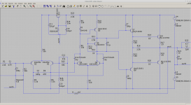
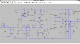
Here's my capture of the factory schematic -- which includes some component values recovered from the unit where the schematic left us to guess. (Sorry, component names here don't match the oem schematic. My bad.)
I'd thought this IPS and VAS design was a "dead end": it'd be nice to improve its performance beyond the ~75dB it's good for, but there's no easy way to add a current mirror or VAS buffer or cascode that would help things. But there's hope for it yet!
Here's my capture of the factory schematic -- which includes some component values recovered from the unit where the schematic left us to guess. (Sorry, component names here don't match the oem schematic. My bad.)
Attachments
Last edited:
Parasound committed some sins with this one.
For one: it uses an incorrect negative feedback takeoff point, where it's likely to get some half-wave rectified error signal into the feedback.
For two: some versions of the HCA-800 II had two pairs of outputs per channel, which is enough to earn the "high current amplifier" moniker. Those could drive tricky 4 ohm loads all day without breaking a sweat. Others, like the one here today, left the factory with only one pair of outputs per channel. Stingy! That's no better than cheesy A/V receivers that promise 100 watts. I wouldn't run this with less than 8 ohm speakers.
The good news is, there are pads for the missing outputs, their base stopper resistors and their ballast resistors. We can add them back.
To reach -100dB distortion performance, we can:
I might also add some filtering on the negative rail for the VAS and IPS, if there's room. PSRR there isn't super great.
- Convert it to triple OPS and adjust the bias spreader to match.
- Cascode the VAS transistor (Q3 on my schematic) so that the VAS transistors see a matching signal at their collectors. Their Cob's will largely cancel, including the nonlinear component of it. To do this we remove one resistor and add Qmod1 in its place.
- Remove the miller cap. Rely on the lead-lag compensation at the IPS tails, and on the lag compensation at the VAS output, and on the lead cap -- all of which get adjusted values. That's enough to produce a nice two-pole loopgain roll-off, with >60dB of feedback in-band, ULGF below 2MHz, and generous stability margins.
I might also add some filtering on the negative rail for the VAS and IPS, if there's room. PSRR there isn't super great.
Attachments
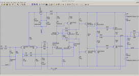
Here's the final circuit as built. Sounds great. There's excellent simulated stability margins with any load, including with a range of current-source loads attached to the output. It's nice to have the 2nd set of outputs on there!
A couple notes on this.
A couple notes on this.
- The 1.5mA current source driving the IPS is a CRD in real life. This improves on the resistive source used originally: the OPS bias current is a function of VAS current which is a function of IPS bias current. With a resistor driving the IPS as in the original design, IPS bias current fluctuates with the input signal level, so output stage bias is poorly controlled. It's not a problem with a purely resistive load, where the output stage always crosses over at 0 output voltage (and thus 0 input voltage); the trouble only shows up with a reactive load.
- The mismatched base-stoppers were due to a shortage of resistors on the shelf, not intentional. Someday I'll get those matched, probably 5.6 is about right for all of them. Meanwhile, this compromises current-sharing a bit, not badly.
Attachments
Q6 is the bias spreader, its collector sees a low voltage.
Q12 is a cascode for Q3. (It ensures that Q3 and Q4 see mirrored collector voltages; we want their Cob's cancel.) Anyway Q12 can see 100V, it must be a high voltage type.
Q12 is a cascode for Q3. (It ensures that Q3 and Q4 see mirrored collector voltages; we want their Cob's cancel.) Anyway Q12 can see 100V, it must be a high voltage type.
Stuff the HV part-type in both positions and get better matched VBE thus better matched emitter voltages thus better matched collector voltages on the diff pair.
Nice circuit. Might have to build one or two... How is your layout? I assume a bit critical without the miller cap? Or is that where C3 and C4 come in?
So did you reaach -100dB? Will emitter resistors in the IPS and VAS improve local linearity thus overall linearity?
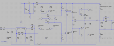
Here's an improved variant of the mod.
The original from comments 3 and 4 has a weakness: it performs well if Q3 and Q4 have matching parasitics, but its distortion performance degrades if they don't. You can see this in spice by replacing either transistor with a different type, like a 2SC3503. Whoops. Of course, we should ideally not depend on precise matching of parts.
This new revision is still easy to build on the original PCB with minimal drilling. It now uses two current-regulator diodes per channel, shown as current sources on the schematic.
In the new version, the VAS is no longer double-sided, it becomes single-sided with a current source load. Neither Q3 nor Q4 see any substantial voltage swing, so the IPS doesn't have to drive any nonlinear Cob or early effect. The Q3/Q4 stage serves as a buffer to isolate the IPS from the nonlinear Cob and early effect of Q5. Together Q3, Q4, and Q5 work effectively as a buffered VAS.
This simulates around -110dB distortion floor into a 4 ohm load. Stability margins are generous, >60 degree phase margin and a full 24dB of gain margin. Note the added capacitor at Cmod5 in parallel with Q5's emitter resistor -- this boosts gain margin. No two solid state devices in the circuit need to be closely balanced to reach these specs. (The IPS tail resistors R803 and R804 should still be balanced to ensure current in the IPS devices is balanced. A 10% error between these resistors degrades distortion performance, but it's still better than -100dB.)
Attachments
The "Parasound" topology shows up in other amplifiers that could be candidates for the same mod.
From the factory, the Pioneer SA-9500 mkII and Pioneer SX-1080 are nearly identical to the Parasound.
The Sanyo JCX-2600K and -2900K receivers use a similar circuit, albeit with a single-ended VAS, that could perhaps be converted to this circuit in-place too. This is getting further afield from a trivial mod, now we're talking about changing several connections.
All those designs are Miller compensated, and to hit 110dB distortion performance that'd have to change. Whereas the lead-lag compensation of the Parasound worked "out of the box" with just a few edits to component values.
i know you changed the circuit quite a bit for the lag compensation design thread. for this version, i'm surprised that you kept R16; i might guess deleting it would lower distortion just a bit.
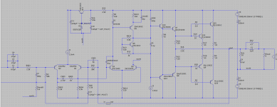
I made some further improvements to this amp -- more easy changes, still on the OEM PCBs.
- Improved PSRR:
- Reintroduced the cascode Q above Q803, but this time the base is grounded.
- Added an R-C filter to lift the IPS tails and VAS. They needn't sit at the negative rail, we can lift them ~10V above it with a beefy filter.
- Improved distortion with better modeling:
- Modeled both "current sources" (really CRDs) as a JFET with a bias resistor. This is probably how CRDs are implemented, though the Semitec CRD datasheets are coy about this. Such a "current source" is neither stiff enough nor linear enough to be ideal as a VAS load. Simulated distortion with the JFET model suffered. It was worse than the -100dB target 🙁
- To fix that I bootstrapped the CRD with another R-C filter. That improves its output impedance by an order of magnitude and puts simulated distortion back where it should be.
- Improved distortion with brute force parts matching:
- Found that distortion suffers if the VAS pair (Q803 and Q804) have a current imbalance. These Semitec CRDs are not graded for tight tolerance, they're within 15% maybe, so VAS load variations can produce an unbalanced VAS pair. I addressed that by tuning R812 on both channels to get a tight balance.
- Another avenue that wouldn't depend so much on parts matching would be to degenerate the IPS and lighten the compensation. That also tolerates imbalanced VAS better. The factory PCB Isn't set up for a degenerated IPS, but if you were laying this out again, it would be a good option.
- Found that distortion suffers if the VAS pair (Q803 and Q804) have a current imbalance. These Semitec CRDs are not graded for tight tolerance, they're within 15% maybe, so VAS load variations can produce an unbalanced VAS pair. I addressed that by tuning R812 on both channels to get a tight balance.
Attachments
Maybe y'all knew this, but I've only learned recently that we must simulate PSRR at both LF and HF.
I thought it was mostly a HF consideration, because the major paths for PS ripple to leak into the signal path are capacitive, eg. Miller caps and parasitic Cob's.
Except that's not true, certainly not for every circuit. Sometimes the path is resistive, eg. parasitic Early effect which affects all freqs equally. This circuit had some Early effect PS ingress, prior to the recent revisions.
Also: PS ripple is probably larger at LF. The big filter caps in a linear power supply will limit the slew rate on the rails, if you assume a given maximum current draw, or maximum charging current. This slew rate can support larger amplitude LF signals than HF signals. So I'd expect that PS ripple has a spectrum that tilts toward LF. (I haven't measured this.)
So it seems like a good idea to simulate PSRR at both LF and HF, and to use larger amplitude signals at LF, up to several volts. That should be realistic, insofar as modeling PS ripple as a sinewave is realistic.
- Home
- Amplifiers
- Solid State
- Improving a Parasound HCA-800 II to -100dB THD