Hi,
I'm working on a Jfet based I/V converter. Open loop, common base, maybe folded cascode if I can get it work.
But based on my simulations, the input impedance is high. A few dozen ohms, compared to the few ohms of a bjt or mos based common gate/base stage, this seems high.
Have I done something wrong, or is this normal with jfets? (making them unappropriate for common gate 🙁)
Thanks
Alex
Presumably you mean common gate and not common base. The input impedance in this case will be the reciprocal of the transconductance. For a 2SK170 running at 5 mA or so, this will typically give 33 ohms input impedance.
I agree with Charles. One reason why a bjt gives much lower input Z here is it's higher transconductance.
Jan Didden
Jan Didden
ok, so I can forget the Jfets for my IV 🙁
you both agree that the input impedance is dependant of the gm
but Mosfets have a lower gm than BJTs, and my sims still show a low input impedance (a few ohms)
no way to have a Jfet IV with a low enough impedance? 🙁
you both agree that the input impedance is dependant of the gm
but Mosfets have a lower gm than BJTs, and my sims still show a low input impedance (a few ohms)
no way to have a Jfet IV with a low enough impedance? 🙁
Bricolo,
Well, why do you insist on a jfet??
it can be done: wrap some feedback around the jfet stage. But I guess that's not exactly what you are waiting for...😀
You want a real novel solution, something others haven't thought about, open loop, excellent quality, simple etc, in other words, worlds best i/v?
Just for you, because I like you:
Get an AD844. Connect the + input to ground. Connect the DAC current output directly to the -input. Put 1k from pin 5 to ground. At pin 6 you take off the signal at 1V/mA. One chip, 1 resistor.
Jan Didden

Is 33 ohms really too high? I remember the old 1541As being happy with anything under 100 ohms or so. In any case, you could always go parallel on the jFETs.
are you talking about this? 😉
http://www.diyaudio.com/forums/showthread.php?s=&threadid=22206&highlight=
http://www.diyaudio.com/forums/showthread.php?s=&threadid=22206&highlight=
SY said:Is 33 ohms really too high? I remember the old 1541As being happy with anything under 100 ohms or so. In any case, you could always go parallel on the jFETs.
the 1541's datasheet telle about 25mV AC swing on its output. Don't know if it is RMS, peak or peak to peak, but if it's peak to peak, it means that the I/V's input impedance must be 6R max
Bricolo said:are you talking about this? 😉
http://www.diyaudio.com/forums/showthread.php?s=&threadid=22206&highlight=
Yes that's it, but I cannot remember seeing it. It looks like I got into that thread after Pedja's posts. So, sorry, no exclusive for you😉 . I'll try to come up with another one...
Anyway, anybody know about the PA630 chip? Basically a SE implementation of the AD844 circuitry, and with two buffers. This was developed and made into an IC by a guy called Wadsworth early 90's on his own time and money. That's the real diy spirit! Brave guy. He made good in the end, sold his remaining inventory + rights + design to Wadia IIRC. They used it in some of their hi-end DACs. Needless to say, I still have a handfull of PA630's here. These are now really collectors items!
Jan Didden
I have something new in mind, but I'm not sure it will work.
Some months ago I proposed a simple I/V based on a current miror. The DAC connected to the "diode" BJT, and 4 similar paralleled BJTs to the output. Advantage: low input impedance, and low output impedance since you can use a lower value I/V resistor because of the current gain.
Now, on my "how to cancel odd order harmonics" thread, there has been some digging about current mirors with gain. Certainly something to dig further.
I cannot distinghuish a fet from a pet
but I have seen that Borberly is doing a Jfet I/V converter.
So it can be done (?) Or is this guy wrong ?
but I have seen that Borberly is doing a Jfet I/V converter.
So it can be done (?) Or is this guy wrong ?
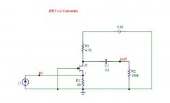
tmblack said:Anyone actually try the one JFET I-V?
Here I use 2SK170BR and 15V supply.
Should work with TDA1541.
Tom
EE
Will the DC-voltage on the source be a problem for a PCM63P converter?
Hi,
I simmed probabely exactly what You look for and it works very well.
Since it will very probabely soon become a commercial product I can´t reveal too much.
Its a common gate stage fed by a current source. Its followed by a N-JFET buffer output stage. This is similar to the idea of. Mr. Hawksford in his AES-paper. He adds some filtering between Input and buffer stage, which I don´t use. With a triple of input JFETs (its very low noise N-JFET but no SK170) I get around 75Ohms input impedance which is near perfect for the PCM 1794 (it translates to ~200mV at the input and ~2.5V at the output) and reduces noise to a very low level. The circuit is of course ´doubled´ to handle the symmetric output of the DAC.
I too prefer the use of simple JFET circuits. To my taste they sound more natural than any complicated or bipolar stage.
jauu
Calvin
- Status
- Not open for further replies.
- Home
- Source & Line
- Digital Line Level
- I/V stage with a common gate Jfet?