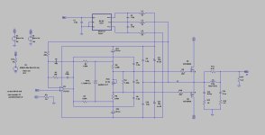
The following circuit was developed for use in a power amplifier that utilizes lateral MOSFETs as output devices. This version is a slight update, since the originally spec'ed BUZ501D/901D devices are no longer available. Theory of operation is straightforward but requires careful selection of component values in order to guarantee stability for all load impedances. IC1 is a high speed current mode op amp that is powered via floating +/- 12V supplies. The use of floating supplies permits the use of an op amp with a reasonable rail voltages that are independent of the MOSFET rail voltages. The op amp inputs consist of In+ from a previous amp stage and V1, which is the unbuffered MOSFET output. As with all op amps, IC1 attempts to generate an output level such that there is (ideally) zero voltage difference between In+ and V1. Therefore the buffer voltage error is dependent upon only the op amp's non-ideal characteristics. Simulations show distortion, (primarily odd harmonics) in the -110 dB range, although such low numbers must be taken with a grain of salt.
The output MOSFETs require a DC bias voltage that sets the idle current. This voltage is derived from IC1 output and the resistor network R4-R8, Pot1, and Vref1. Constant current sources CR1/CR2 effectively isolate the op amp rail voltages from the bias voltage applied to the MOSFETs. Vref1 generates a precision 2.5V that is divided by R6-R8 and Pot1. The resulting drive voltages applied to the MOSFETs are therefore IC1 output +/- 0.5 * the voltage across Pot1. Capacitors C6-C8 provide an AC path between IC1 output and the MOSFET gates.
The cutoff frequencies of both IC1 and the MOSFETs are very high, in the 20-100 MHz range. As such, it is necessary to carefully consider compensation and load decoupling networks. C4/C5 and R1/R2 set the active stage roll-off in the 3 MHz range. Selecting a different op amp or changing the compensation network can result in a lower cutoff frequency at the cost of higher distortion. As is often the case, there exists a tradeoff between distortion and stability. If the load on the MOSFETs were always resistive the previous compensation network would suffice. However such is not usually the case, hence the need for the load decoupling network. Simulations show, for the values given, that the buffer is stable for all R/C output loads. For real-life loads the load decoupling network is mandatory.
MOSFET rail voltages are shown as +/- 50V, but higher or lower voltages can be supported. A single pair of MOSFETs is shown, but multiple pairs can be used, especially for higher rail voltages. For the amplifier I am designing each channel supports 6 n-channel and 6 p-channel devices and, for +/- 70V rails, is capable of approx 500W into 4 ohms.
Attachments
So was it built and tested?"The following circuit was developed for use in a power amplifier that utilizes lateral MOSFETs as output devices."
Thanks.
This is the first amp I've seen that uses floating auxiliary supplies for an opamp that drives lateral MOSFETs without some driver transistors.
Well done! In my experience it is not easy to get this arrangement stable at HF.
Is the opamp on the far panel board?
Also was there a voltage gain board in this case, or a separate unit?
Was the amp manufactured and reviewed somewhere?
Cheers, IanH
Shown below is a spare Rev 1.0 gain stage/MOSFET driver PCB. This is the PCB mounted to the amp front panel. The rectangular island on the right hand side of the PCB is the MOSFET gain stage. DC/DC converters are located off-board.
To my knowledge, no commercially available amplifiers utilize this particular topology. My motivation for placing the MOSFETs and driver in a separate unity gain stage was to relax the requirements of the voltage gain stage, requiring it to drive into an essentially open circuit, such that the voltage gain feedback path is independent of the load. In this regard, the amp topology can be said to have no GFB, but have rather two separate feedback loops.
Regarding HF stability, you are correct. I had to lower the MOSFETs' effective Ft in order for the Rev 1.0 output stage to be stable. The second Rev takes steps to improve HF stability. These include locating the MOSFET driver circuits and DC/DC converters directly on each of the two output PCBs, even though this entails duplicating circuitry. The critical factor is to minimize the inductance between the op amp driver and the MOSFETs, particularly on the virtual ground path labeled V1 on the previous schematic. Simulations showed that even a 1 uH inductance in this path was sufficient to induce instability.
Attachments

A design and build to envy.. Im surprised it works. Why not use a bootstrapped resistor zener supply for the opamp?
The 1uH you mention may need to be less in practice. Did you use the latest lateral VDMOS models? There are some at the Bordodynov site:
http://www.bordodynov.ltwiki.org/
This site https://www.tonestack.net/articles/cables/speaker-cable-guide.html gives zip cord inductance as 0.6 to 0.7 uH/m. So maybe you can get away with 10 cm or 20cm interboard connects.
I notice C4 18pF connects from U1 output to inverting input. The datasheet says never connect a capacitor across this path. It seems you have found an exception to their rule, somehow?
Overall, what's the takeaway(s) from your design/topology? Please explain.
Is it - don't do it like this, unless you feel very lucky? Doug Self and Bob Cordell say they stick to the topology that is the easiest to get to work.
The choice of circuit topology and components was driven by the original requirements for a 500W lab amp that could drive both resistive and reactive loads and required a DC-1 MHz bandwidth. In use it was driven by an AWG into a voltage gain stage and then into the MOSFET buffer. It so turned out that the design also proved amenable for audio use, showing excellent drive and distortion characteristics.
I'll address some of your above listed concerns below.
A previous reviewer suggested using a bootstrapped Zener to the +/- rails. I chose DC/DC converters because they permit gate drive signals that are referenced to the output drive voltage and can therefore produce MOSFET drive voltages above the +/- MOSFET rail voltages. This, of course, assumes that the maximum input drive voltage is >= to the MOSFET rail voltage, which it is. DC/DC converters offer excellent input-output isolation, consisting mainly of a low capacitance.
LT1223: It it true that the LT1223 datasheet cautions against putting a cap between the inverting output and the output, but that is for a conventional topology. Omitting C4 produces a sharp peak in the 40 MHz range; adding C4 eliminates this peak. R2 and C5 are likewise required to eliminate a peak in the 5.0-10.0 MHz range. As I mentioned previously, load isolation is important, and the output network is essential.
Regarding the choice of the LT1223: it turns out that other, lower BW op amps, will work as well, albeit yielding higher distortion at a lower overall BW. As is usual, there is a tradeoff between low distortion and stability. The LT1223 output current is spec'ed at 50 ma (min), which turns out to be overkill. MOSFETs present a capacitive load such that the required drive current is a function of capacitance * amplitude * frequency and is quite modest. For example, a 20 kHz 60V peak output voltage driving 6 MOSFETs requires a peak drive current of 6 mA This number is well within the range of many op amps.
I regard the amp design in a manner similar to light aircraft. An Extra EA-300 will do things that a Cessna 172 will not. A pilot would ill be advised to attempt flat spins and hammerheads in a 172. That requires a high performance aircraft and an experienced pilot. In a similar vein, I would not recommend this design for a beginner, but for an experienced electrical engineer, it is not that difficult. As regards luck, I would say "no". The design was based on a successful previous example, and all subsequent changes were carefully thought out and simulated at many corner cases.
Attachments


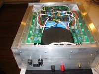
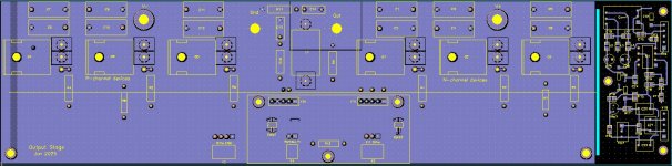
Shown below is the proposed output stage PCB, two of which are required for each amplifier. Hopefully the layout details will resolve some of the above mentioned questions.
Each PCB connects three n-Ch and three P-ch lateral MOSFETs. (Exicon P/N EXF20N20 and ECN20P20, respectively). The MOSFETs mount on the back side of the PCB while all other components mount on the front side.
One major difference between this and the previous design is locating the MOSFET drive circuit on the output PCB. In the original design this circuit resided on the gain stage PCB, and wiring inductance between the two was a problem. The drive circuit is located on a small PCB on the right that plugs into the main PCB via two strip connectors. I chose to put the drive circuitry on a separate PCB because doing so minimizes cuts in the main PCB top layer, which is the ground plane. Vdd/Vss power and ground connect via 2x 14 AWG stranded wire to a separate power PCB, with maximum wire length of 8 inches. Twelve 0.47 uF caps tie Vdd and Vss to the ground plane, minimizing the inductance between rails and the MOSFET drain terminals.
Large through-hole gate resistors are used because they minimize cuts in the MOSFET source plane. Simulations show that minimizing inductance between this plane and Drive_Com net on the drive PCB is critical for HF stability.
Two MOSFET relays on the main PCB are part of the overload protection circuitry. In event of an overload the relays turn off, and the MOSFETs turn off in approx 100 uS.
Attachments

- Home
- Amplifiers
- Solid State
- High Current Output Buffer for Monoblock Power Amplifier