Hi,
I recently got a Yamaha A-500 integrated amp made in 1982. I cleaned the pots, switches and contacts, and verified bias is to specs. The amp sounds fine and plays quite loud without noticeable distortion. It runs warm but not excessively so; pretty much like other similar amps I had. No component shows any sign of damage.
The only thing is that it has 127mV of DC on L channel, and -226mV on R. Loading it with my 6-ohm speakers brings this down to 117mV and -210mV, respectively.
Given it's age, and that a poor electrolytic cap may be the cause, I'm going to replace all electrolytics. In case the recap does not solve the problem, I'll look into replacing the matched input transistors or add resistor/trim to compensate. However, I'm not sure which are the input transistors or where to add resistance. I uploaded a pic of the schematic; not sure how clear it will display. Service manual is too large to upload; it can be found here Yamaha A-500 - Manual - Stereo Integrated Amplifier - HiFi Engine
Looking at the main amp section right channel, would the matched input pair be TR104-TR106, TR108-TR110 or TR116-TR118? And where would I add resistance? To the correct pair's emitters? Would you advice adding x ohms resistors or trims?
Thanks in advance for your help.
Bill
Attachments
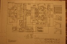
Sounds like a plan. The input LTP are TR107/TR109 and TR108/TR110.
Don't see any easy way to adjust the offset, you would have to leak a bit of current into one of the LTP bases.
Don't see any easy way to adjust the offset, you would have to leak a bit of current into one of the LTP bases.
I dunno if I want to sign up at HiFi Engine for this. But from the jpeg, looks like you have a couple source resistors for the JFETs that could be a trim pot, maybe temporary to find fixed values. IE the sum of the two should remain the same.
There is also a pair or pull-up resistors between the JFETs and the BJT diff-amp that could be tweaked.
There is something strange between the VBE multiplier and drivers that could be important but I can't make it out from the low-res JPG. Maybe this amp puts the tone controls in the power amp, which is not a great idea.
First check for me would be to scope the output and make sure the DC offset isn't in fact any kind of low level asymetric HF instability. Its odd for both channels to have a moderate offset of this magnitude.
Temporarily (or not) install a multi-turn 100R trimmer in parallel to input J-fets (TR103/TR105) source resistors (R169/R171), trimmer ends between sources and resistors, wiper to R173, set trimmer to midpoint. Disconnect all sources and speakers form amp, turn it on, let it worm up for 30 min., check output DC offset and adjust trimmer for minimum offset, do the same after another 30 min. Adjust trimmer very, very slowly with an aye on multimeter!

I would replace the input FETS with a DUAL FET or add a DC offset the input stage. By modifying the Source Resistor the Gain will change and other problems may raise their heads. If you make a +/- 0.6 volt and place a pot across it and feed it to the input gate resistor it would give you a DC offset to correct for poor FET matching. Any Output DC >+/- 10 mv is what I not feel good with. With 200mv and a 4 ohm speaker the idle current in the speaker is >50ma. @ no signal.
Duke
Duke
The 100 ohm trims suggested by aparatusonitus work, but only bring down the dc to 99mV and -203mV. Do I need larger or smaller value trims to lower dc further?
I swapped a FET from each pair and now I have R at -56mV and L hovering within +/- 2mV around 0 (with the trims* turned all the way to one side).
Not bad!
Should I worry about 56mV into my 40ohm headphones?
*100ohm 25-turn Bourne.
Not bad!
Should I worry about 56mV into my 40ohm headphones?
*100ohm 25-turn Bourne.
personally, before all that, I would have a test with its original mains voltage and variac ...
to see.
to see.
The headphone feed should be padded down with resistors (which I can't make out on the diagram) which will reduce the open circuit offset voltage measured at the phones socket to a low level once the phones are connected.
- Status
- Not open for further replies.
- Home
- Amplifiers
- Solid State
- Help with DC offset on Yamaha A-500 amp