I have been studying but i could not find the solution.....yet!
If you want to help me, them post something.
Videos will explain you the problem, please, they are below.
Sorry about the english (eingrish or englönder) and portuguese all together:
https://www.youtube.com/watch?v=YitLXEF9U8w
https://www.youtube.com/watch?v=H3MDn3uXIkU
A happy new year to all forum friends🙂.... to the non very good friends, i wish you just a new year.😱
regards,
Carlos
Without having seen your youtubes, I question if you know the article of M. J. Hawksford "Optimization of the Amplified-Diode Bias Circuit for Audio Amplifiers"?
Greetings, Marc.
Greetings, Marc.
I see.....something Horowitz said in the seventies
It is not exaclty that kind of improvement i am searching for.
Sorry, you gonna need to listen my bad english....please do not laugh🙂
regards,
Carlos
It is not exaclty that kind of improvement i am searching for.
Sorry, you gonna need to listen my bad english....please do not laugh🙂
regards,
Carlos
Hi Carlos
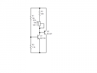
I think the issue you are faced with is some mis-match between the MJL's and BD139 base-emitter voltages. The standard bias circuit is actually based on an incorrect premise and is no good, but has worked well for me using BD139/2N3055, BD140/MJ2955 output set with a BD139 stabiliser. First comment, I assume the bias stabiliser is mounted on the same heatsink as the driver/output pair. This is essential.
The standard circuit is WRONG because it adjusts the multiplication factor of the Vbe to set the quiescent current. So if your bias regulator has 0.65V but the driver and output transistors only have 0.625V the bias voltage needed is 2.5V but compared with the bias transistor Vbe this is only 3.85 times, so the ratio is never going to match the number of Vbe's to balance.
My proposal is to use a dual transistor bias regulator. The ratio is set to 4 exactly with the first two resistors (10k:3.3k = 13.3/3.3=4) and the "trick" is to change the CURRENT in the bias transistor until the Vbe matches the output set. The BD139 should be mounted on the same heatsink etc. but the PNP transistor does not have to be.
If the bias overcompensates the ratio can be reduced or undercompensates the ratio can be increased by changing the division ratio resistors.
I've posted this circuit before, but not everyone in this forum remembers or sees it if it is a different thread.
Hope this helps.
John
Attachments
Thank you dear John..... very helpfull schematic and for sure i gonna try it
Yes, i gonna do it.
But maybe i was not that clear....my problem is more related the modulation of audio into the system...the fact that when the signal is driving the positive rail it produces a bigger voltage (naturally has current as consequence when face zener effect of drivers and output transistors) reducing the voltage to drive the negative rail that gonna have transistors off...this is my main problem, to keep them on all the time... to have a bias voltage that senses the audio modulator entering and compensates in order not to cut out the negative rail.
Oh!...my english was weak!, i thought i was clear about that...or video is too much long and people cannot watch it entirelly.... will make a new one... a very short one.
Thank you very much dear John.
regards,
Carlos
Video answer to you dear John Ellis
Here you have it:
https://www.youtube.com/watch?v=gl8AtRu3q_Y
I hope more clear now.
regards,
Carlos
Here you have it:
https://www.youtube.com/watch?v=gl8AtRu3q_Y
I hope more clear now.
regards,
Carlos
If I read the posts correctly, you are looking for an auto-bias circuit for class AB amplifiers. This has been done here in the past, by members such as Edmond Stuart but you won't like the complexity of the circuits.
He has already outlined the problem, posted solutions in several threads and provided a practical design here: Auto Bias part II
However, your simulation seems to be the problem you show in the video link. The bias measurements do not distinguish DC from AC. It is necessary to filter the DC component from the audio signal to measure it as DC alone but the constant difference of the DC bias voltage to the signal voltage will always be there.
Even with a perfect bias generator, any bias current you estimate this way, will look similar.
Yes Ian Finch, you are rigth, i have to filter, it is confused
I gonna read the text.
Thank you very much.
I cannot contact this link, gonna try latter:
http://www.data-odyssey.nl/AutoBias_II.html
regards,
Carlos
I gonna read the text.
Thank you very much.
I cannot contact this link, gonna try latter:
http://www.data-odyssey.nl/AutoBias_II.html
regards,
Carlos
RJMI, thank you.
I could not make contact with the link you have provided.
Gonna try it once again latter.
regards,
Carlos
I could not make contact with the link you have provided.
Gonna try it once again latter.
regards,
Carlos
Dear PituWilson, already downloaded your Madrigal paper
I will read it.
Thank you very much,
regards,
Carlos
I will read it.
Thank you very much,
regards,
Carlos
Found!... circuit already found
One from Dunlop, published in this same forum back 2009
Another one sent by email.... a Pioneer non switching amplifier.
So, i am satisfied as i have something to do in my workbench, something to
tune and develop.....i may return showing you results end of January or february 2016.
Video attached show these amplifiers and explains something basic about it... i am still trying to understand it
deeply.
https://www.youtube.com/watch?v=5PvyJTQM5h8
Thank you all,
regards,
Carlos
1) Andrew C. Russell uses low voltage opamps to establish a high accuracy 2-slope Vbe vs. Temp bias.
Ideas on Temperature Compensation for Emitter Follower Triples in Class AB Audio Amplifiers
Some Ideas on Temperature Compensation for Audio Amplifier EF Triples
-----
2) Plateau Bias is superior to Sliding Bias for extending Class-A bias range.
Some amp critics report hearing artifacts of rapid sonic "high-bias <--> low bias" changes when a dynamic sliding bias circuit is used to provide "some" Class-A bias with minimum initial static bias .
Krell VFA amps use a Plateau Bias patent (5,331,291) which senses large current demands at the output and at the pre-driver, and increases bias current for a short period before testing for safe bias reductions. Krell has recently patented iBias which uses a microprocessor to control the bias algorithm for Krells new CFA amps.
Carlos one solution is to bias the bias cicuit to a supply, such way that when the output goes down it increases the total bias. Also with increasing output, the bias has to increase. This can be done with an extra bias resistor to each supply. Similarly to 2 slope protection systems, really very similar.
Jan
Jan
Thank you friends, already found what i was searching for
Good idea Jan Didden.
Linesource....too much complicated solution to my old single neuronium.
Look at me dear line.... an old bugger, memory may be 16k alike Sinclair Z80...not fast nor clever anymore.
Things goes changing fellows..... i am another man..... you may recognize
me because i still like girls...a lot!... their hardware can be fets, bjts, Igtbs, chips, tubes...no problems about details.
regards,
Carlos
Attachments


Last edited:
You may think i am still searching for a solution
Negative, i have already found and i have published in my last video attached:
https://www.youtube.com/watch?v=5PvyJTQM5h8
Twi circuits interest me to research on them....the Dunlap circuit, from this same forum down 2009 and another one people sent me using my email, a Pioneer.
So, thank you all, but my search is already finished...i feel myself satisfied and once again thank you all by the cooperation.
regards,
Carlos
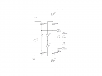
Carlos,
I think you are looking for a solution which keeps the transistors always on - not necessarily a sliding bias, but a system that uses a "dual bias" approach. Blomley suggested a circuit many years ago in Wireless World, as it was. He separated the output bias regulator from the driver and used a diode splitter to steer current from the signal to the output/driver stages.
One approach I have tried is what I call a "double bias circuit". This uses a standard bias method (using the "proper" Vbe multiplier as I outlined and others have pointed out are mentioned by D Self) but with THREE circuits. One forms the regular bias stabiliser; the other two work from separate current-driven bias supplies between the rails and centre point. The two bias circuits are joined by diodes (see illustration).
THe idea is that when the signal current reduces the bias is maintained by the auxiliary circuits.
What I found is that the concept works, but the main issue was setting it up. With three bias controls, it is necessary to start the adjustment with the aux bias set to zero and first set the quiescent current with the main adjuster. Then, carefully increasing both aux bias currents until the quiescent current JUST starts to increase, maintaining a balance for zero output (this needed three meters connected up).
I also found that the main problem with crossover distortion is at high frequencies. The stored charge in the ouput transistor bases needs to be removed quickly or this acts as its own sliding bias. FOr this reason, I have had better results reducing the base-to-base resistor in the DRIVERS, using triples to increse the available drive, and then just a standard class AB system works OK.
In this approach, reducing the base-to-base resistors to keep the driver(s) in Class A means that only the output transistors have to work in Class B.
Regards
John
Attachments
- Status
- Not open for further replies.
- Home
- Amplifiers
- Solid State
- Help me to improve our prehistoric VBE multiplier biasing system