Hi guys
a few months ago an old amp landed in my house with unknown origins! there seens to be absolutly nothing about this unit online!
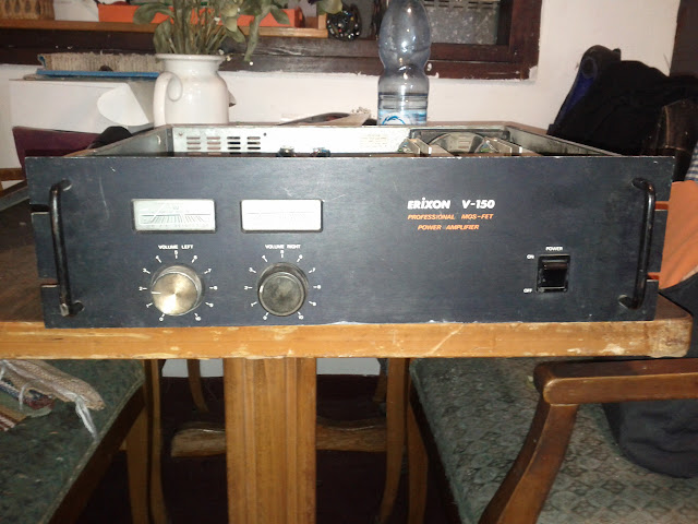
this is the unit:
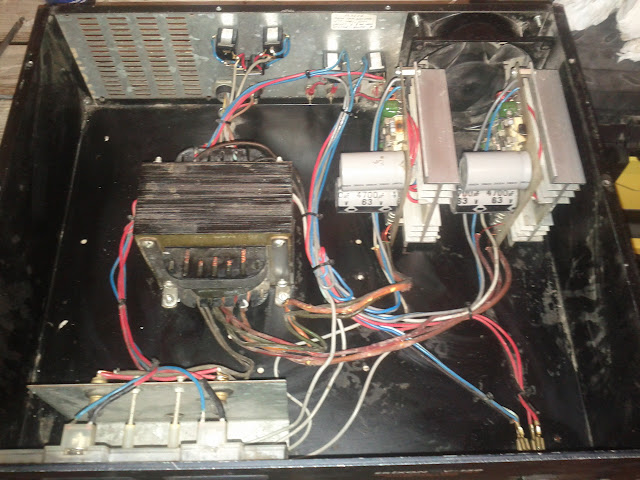
and the inside (after some serious cleaning!):
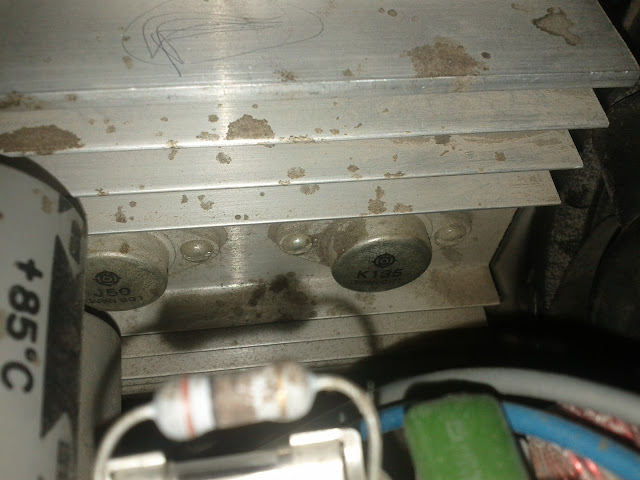
and the mosfets:
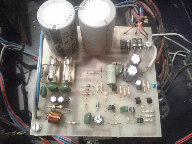
and finally, the board itself:
after alot of reaserch, a friend of mine said it might be an elektor kit from the 80 that was factory produced, so i thought ill check here with you guys and hopefully someone will have an idea on were i can find more info on the unit, its schematics and bias..
also, i allready orderd new caps
for it because i plan to rebuild it - it sound very nice through my Tannoys DC!!
thank you all for you time!
Omri
a few months ago an old amp landed in my house with unknown origins! there seens to be absolutly nothing about this unit online!
this is the unit:
and the inside (after some serious cleaning!):
and the mosfets:
and finally, the board itself:
after alot of reaserch, a friend of mine said it might be an elektor kit from the 80 that was factory produced, so i thought ill check here with you guys and hopefully someone will have an idea on were i can find more info on the unit, its schematics and bias..
also, i allready orderd new caps
for it because i plan to rebuild it - it sound very nice through my Tannoys DC!!
thank you all for you time!
Omri
problem is.. i cant find any form of schematics, which will make the recap procces that much more difficult! i really hoped its based on an elektor kit 😕
Very difficult. You mat try to make a wiring handmade, or if you only need to replace the caps, then with the use the same rating of capacitance (or greater) and voltage, and making a mark to identify the polarity of the old cap and putting new in the same way, there must not be any trouble.
I remark to u, don't use too big voltage for the caps. If, you have a 40V in some point, use 50 or 63V, but no 100 or more, because such high difference not only are bulky and more expensive, their performance is also lower than a nearer WV.
I remark to u, don't use too big voltage for the caps. If, you have a 40V in some point, use 50 or 63V, but no 100 or more, because such high difference not only are bulky and more expensive, their performance is also lower than a nearer WV.
Wow, looks like an awful implementation of the Hitachi MOSFET app note. 2SK135/2SJ50 were the Hitachi MOSFETs of the time.
The circuit is probably 80W/8 ohms, really those heatsinks are too small but acceptable with the fan, perhaps.
The Hitachi circuit is crude and can be much improved upon.
The circuit is probably 80W/8 ohms, really those heatsinks are too small but acceptable with the fan, perhaps.
The Hitachi circuit is crude and can be much improved upon.
well to be honest, i have never practiced or learned any form of electronics, let alone build an amp so the task of rebuilding the circuit around those mosfets is a daunting task for me right now.. a recap how ever seems like something i can handle.
i did connect this amp before, and even though the caps were at terrible state it sounded quite nice, with good imaging and a very full sound! i look at this project as a fun learning experience and not much more and if it ends up sounding good - i wont complain!
i did connect this amp before, and even though the caps were at terrible state it sounded quite nice, with good imaging and a very full sound! i look at this project as a fun learning experience and not much more and if it ends up sounding good - i wont complain!
If you really cannot find a schematic then by the looks of of the images you've posted up, the circuit board should not be that difficult to reverse engineer. If this is too much of a task, PM me & I'll quite happily do this for you and post the resulting schematic up on this thread. To enable me to do this, I will need a hi-res picture of the bottom & top of the assembled circuit board(s).
Should be an interesting exercise.
Andy
Should be an interesting exercise.
Andy
If you really cannot find a schematic then by the looks of of the images you've posted up, the circuit board should not be that difficult to reverse engineer. If this is too much of a task, PM me & I'll quite happily do this for you and post the resulting schematic up on this thread. To enable me to do this, I will need a hi-res picture of the bottom & top of the assembled circuit board(s).
Should be an interesting exercise.
Andy
that is a wonderfull offer underwurlde!! i will PM you with a link to the hires pics ones i get back home from work! who knows, maybe ill even find out what the bias this way😀
What issues do you anticipate in a recapping exercise anyway? This is a replacement task, done like Lego if you simply replace just the electrolytic types with similar ones. Given that the grades marked will no longer be available, you need only select a common (not the smallest and cheapest) type from reputable manufacturers like Panasonic, Nichicon, Elna, UCC etc.
The parameters most important are spacings for leads passing through the PCB and to match or exceed the marked capacitance and voltages by say, no more than 50%. Sure, make sure they will fit for diameter and height but modern caps tend to be much smaller than even their 1980s predecessors. Just get the lead polarity right!
How hard is that?
Bias, BTW, was routinely set low on early Hitachi derivative designs which usually sounded poor. It is not critical but may benefit from being set higher at 80-100 mA, as measured by calculating from a voltage measured across (one of) the large source resistors. You need a reasonable quality DMM for this and verify that the current you set remains stable with no signal or speaker fitted. The amplifier may run considerably warmer with this amount of bias - check heatsink temp is not burning to the touch after warm-up.
Last edited:
Anyone who has ever built or serviced a MOSFET Hafler kit knows what your amp is. A David Hafler design clone with Home Lighting Dimmer Knobs added for style. . You could call it a DH-100 clone. I remember seeing a few similar amps like this sold in the 1980s through DIY channels of those days like the back of Radio Electronics and such classifieds. Both as assembled and as kits.
These Hafler schematic excerpts show a basic similar AB Design (not exactly the same) - similar theory tho.... Yours use different but probably decent MOSFETs and obviously less output stages than a DH-500 and lower power all around and less need for all that DC power too. I think the DH-500 design has a total of 12 output MOSFETs for a total 255W/Ch into 8Ohms. How many does this have? I'll bet even with your cheaper Hitachi MOSFETs and small caps this amp design does achieve basic good clarity and dynamics for what it cost originally as a kit. MOSFET design amps were always a good value. I credit that to David Hafler and how he applied it. That DH-500 box is genius in a kit. This amp does looks like crap but might sound good.
Subtract the Hafler speaker protection circuit and it's relay, the fan speed control circuit, and several more output MOSFETs and what you have starts to look a lot like this schematic of a Hafler preamp driver board section attached to the outside of the fan cooled Heatsink Cube with MOSFETs. You'll find that your boards are a combo board of this similar design in a dual mono attempt. Again, the limitations of your PCB solder traces limits how far away you want to put the 'better than" size replacement caps if necessary and what improvements you can easily perform. You could probably get away with almost doubling the existing cap values to try and keep them in the same mounting location so you don't have to run PS power leads to new caps on an ***-on board. I would avoid multiple paralleled caps on this one. Always strap, glue or bracket the caps down to the board just in case as far as safety. I like to wear eye protection myself when working on these.
In theory this bias design allows for cascading or adding multiple stages of output MOSFETS to the same basic circuit to increase output current sourcing thus increasing power output assuming they can be accommodated on a heatsink and the power supply could handle it, etc. . Not that I would try this on what you have here. It will melt.

I don't think the downloadable Hafler DH-500 manual has the parts list for cross-referencing these capacitor values? They also don't discuss biasing or testing the bias voltage in that manual either ...tisk...tisk. Hope this helps. Get a Hafler.

These Hafler schematic excerpts show a basic similar AB Design (not exactly the same) - similar theory tho.... Yours use different but probably decent MOSFETs and obviously less output stages than a DH-500 and lower power all around and less need for all that DC power too. I think the DH-500 design has a total of 12 output MOSFETs for a total 255W/Ch into 8Ohms. How many does this have? I'll bet even with your cheaper Hitachi MOSFETs and small caps this amp design does achieve basic good clarity and dynamics for what it cost originally as a kit. MOSFET design amps were always a good value. I credit that to David Hafler and how he applied it. That DH-500 box is genius in a kit. This amp does looks like crap but might sound good.
Subtract the Hafler speaker protection circuit and it's relay, the fan speed control circuit, and several more output MOSFETs and what you have starts to look a lot like this schematic of a Hafler preamp driver board section attached to the outside of the fan cooled Heatsink Cube with MOSFETs. You'll find that your boards are a combo board of this similar design in a dual mono attempt. Again, the limitations of your PCB solder traces limits how far away you want to put the 'better than" size replacement caps if necessary and what improvements you can easily perform. You could probably get away with almost doubling the existing cap values to try and keep them in the same mounting location so you don't have to run PS power leads to new caps on an ***-on board. I would avoid multiple paralleled caps on this one. Always strap, glue or bracket the caps down to the board just in case as far as safety. I like to wear eye protection myself when working on these.
In theory this bias design allows for cascading or adding multiple stages of output MOSFETS to the same basic circuit to increase output current sourcing thus increasing power output assuming they can be accommodated on a heatsink and the power supply could handle it, etc. . Not that I would try this on what you have here. It will melt.
I don't think the downloadable Hafler DH-500 manual has the parts list for cross-referencing these capacitor values? They also don't discuss biasing or testing the bias voltage in that manual either ...tisk...tisk. Hope this helps. Get a Hafler.
Hi,
FWIW there appears to be no grasp of "hi fidelity" wiring practise in that amplifier.
Its also got unshrouded mains spade connectors which is illegal AFAIK.
rgds, sreten.
FWIW there appears to be no grasp of "hi fidelity" wiring practise in that amplifier.
Its also got unshrouded mains spade connectors which is illegal AFAIK.
rgds, sreten.
Last edited:
wow guys thank you so much for your help!!
i sat down to make a cap list which ill order today through digikey, it seems that all the values and sizes are availabe 😀
i also "redesigned" the inside so later on i will be able to get rid of the fan and install bigger heatsinks:
in the end, i took a bunch of hires photos of the circuites found in this album:
https://picasaweb.google.com/111109714414066634160/Recap
i am aware that a recap job is very much like lego and i dont anticipate any major problems from that procces but it is new and rather exciting for me considering i always stayed away from any form of electronics work.. i just hope this is not going to prove itself as a terrible waste of time considering how not impressed you guys are with the design of this amp 😕
wood cutting and metal welding are my cup of tea.. and just for refference so you guys wont think im completely incompitent, my Tannoys DC (DIY...):


😎
i sat down to make a cap list which ill order today through digikey, it seems that all the values and sizes are availabe 😀
i also "redesigned" the inside so later on i will be able to get rid of the fan and install bigger heatsinks:
An externally hosted image should be here but it was not working when we last tested it.
in the end, i took a bunch of hires photos of the circuites found in this album:
https://picasaweb.google.com/111109714414066634160/Recap
i am aware that a recap job is very much like lego and i dont anticipate any major problems from that procces but it is new and rather exciting for me considering i always stayed away from any form of electronics work.. i just hope this is not going to prove itself as a terrible waste of time considering how not impressed you guys are with the design of this amp 😕
wood cutting and metal welding are my cup of tea.. and just for refference so you guys wont think im completely incompitent, my Tannoys DC (DIY...):
😎
Looking at pictures 3 through 6 in your photo album reveals some former or perhaps current problems. The resistor next to the output inductor has been overheated and should be replaced. Also of note the resistor next to the fuse holders has obviously been replaced as the original looks to have burnt by the marks on the board and fuse holder. Pic 24 of the bottom side shows evidence of several parts being replaced as well. Before hooking this thing back up to such expensive speakers you really need to thoroughly check voltages and operation of the amplifier using a cheap test speaker after it being powered on for some time to see if there will be any faults.
Last edited:
From what I can make out, this is what you have:

Power Supply:

Very similar to the schematic shown here: http://www.novagraph.com/examples/mosfet.html
Andy
Power Supply:
Very similar to the schematic shown here: http://www.novagraph.com/examples/mosfet.html
Andy
Last edited:
Oh, & placement of components as I've drawn it above:

No doubt there are myriad ways of improving your amplifier too.
Andy
No doubt there are myriad ways of improving your amplifier too.
Andy
Errata:
i) I suspect that 680R R20 should go to -Ve rail and not GND as I've drawn it.
ii) I've got TR6 upside-down!
Apologies! 🙄
Andy
i) I suspect that 680R R20 should go to -Ve rail and not GND as I've drawn it.
ii) I've got TR6 upside-down!
Apologies! 🙄
Andy
Nice work on that schemo Underwurlde ! This might be a good time to take some voltage measurements around the VR1 pots for both channels at idle and talk about reverse engineering/calculating the bias currents and confirm proper bias. I wouldn't mess with adjusting those bias adj. pots just yet. These designs are sometimes a bit specific as far as the bias current for safety margin using the selected output MOSFETS although they will work in a broader range. I've been away from my calculator too long to calculate the current mirror bias properly here but I'm sure your fellow DIY'ers here eat this stuff up. Its a common problem confirming and adjusting bias on UFOs without any documentation. Leaving the pots the way you received it is one good solution. I like to at least confirm all associated voltages right vs. left are close to start with so I know I don't have a 'run-away' or possibly over-heating improperly biased channel. When I buy or service old S.S. amps I often touch the right and left channel heatsinks to check that they are equally warm when idle.
underwurlde you are the man!!! sorry it took me so long to reply but its been crazy at my work place.. hopefully the caps i ordered will be here soon and ill have a good excuse to give myself some time off 🙂
the schematics you made will surely become more then handy in the procces, even though a recap job of this scale should be super simple, as i stated before - it is my first venture in to the world of electronics and i can use all the help i get (and i get a bunch on this website!).
now i need to keep my fingers crossed that this unit will turn out nice.. and it has quite the competition right now! my 1968 AR amp just came back from the repair shop and it sound absolutly amazing with my large DIY Tannoys!!
the reason i have a good feeling about this unit is the fact that every mosfet design ive seen up until now was super simple in design and from my understanding the best mosfet design are acutally the most simple ones.. but thats just my understanding. also, from what i read, the k135 and j50 and highly regarded. and on that note, you guys say that there are alot of changes that can be made on this unit.. what sort of changes are those? does it mean ill have to intirelly chance the circuit and just keep the power supply and mosfets or are this simple changes that could be made on the excsiting pcb? also, will i benefit from a rewire work? heck.. i would love to turn this unit into a little project and "Pimp" it good, but does it have good enough of a base structure?
The resistor next to the inductor that is burnt... check the inductor. the resistor should have 0 ohms if the inductor is fine. They are both in parallel, and for that resistor to burn, the inductor must leave the circuit.
The resistor near the fuse holder looks similar to the resistor in the DH-120. It creates a rock solid voltage, and creates a LOT of heat, so elevating it is a good idea.
The resistor near the fuse holder looks similar to the resistor in the DH-120. It creates a rock solid voltage, and creates a LOT of heat, so elevating it is a good idea.
- Status
- Not open for further replies.
- Home
- Amplifiers
- Solid State
- help me identify this amp