I'm currently building a IV stage for my PCM1794 DAC I used the FETaudio IV stage as a reference and am trying to improve on it, I want to use only TO-92 transistors and a 15V+/- rail. I have used ltspice to simulate the circuit and cannot decide if I should use BJT or JFET in the output buffer and differential amp, which would be best for that position, also what bias currents are best for the circuits? help would be greatly appreciated, i'm looking for the best possible performance and lowest distortion.
the LT1009 2.5v reference will be TL431 in real life.
how much power can a to-92 transistor dissipate in a enclosed chassis the highest dissipation in the circuit is 119mW is that too much for a TO-92 transistor?
the LT1009 2.5v reference will be TL431 in real life.
how much power can a to-92 transistor dissipate in a enclosed chassis the highest dissipation in the circuit is 119mW is that too much for a TO-92 transistor?
Attachments

Hi,
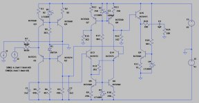
Your schematic contains several failures.
- DAC currents incorrect, DACs centre current is missing
- D1, D2 wrong circuit, wrong parts. A simple 1N4148 anode connected to Q1/Q2s base suffices
- Q3/Q4 should be PNPs like Q7/Q8 in the second stage
- U1/R5 position switched, compare to second stage again.
No failures but points one may think about:
- C1, C2 quite large
- U1,U2,U3 may be replaced by cheap and simple LEDs instead
- second stage is mainly used to level translate the signal voltage of the 1st stage so that a N-JFET can be used as buffer. The complete 2nd stage would become obsolete if the 1st stage were not a PNP common Base stage but NPN
- overly complex curent sink Q9-Q12/R21,22. The single JFET buffer is so high in THD, that a similar simple CCS would suffice. Besides, it probabely spoils any THD possible benefit of the leading stages.
Also, complex CCS tend to oscillate.
Have a read in this thread "Current differential to voltage line level from PCM1794 et al" and see #52. 😉
jauu
Calvin
thanks for the help, are there any full proof circuits for the PCM1794 that can do differential to single-ended that is discrete non-feedback and uses to-92 parts?
Hi,
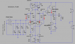
The second stage of #4 is a differential voltage gain stage with its gain set by the relation of R15/R16 to R14. Its used here rather as level translator with two outputs which may be taken off differentially or SE. The level translation was required due to the following NJFET source follower, resp. NPN emitter follower.
If You replace the NPN emitter follower Q15 by an PNP and the NPN current sink Q9 by a PNP current source You can omit with the second stage alltogether.
Connect Q15 either to R4/C1 or R3/C2.
That'd have the potential for a very good sounding IV and Buffer already.
THD will be ok, but not very low. If You add NPNs to Q1/Q2 to form a CFP and do similar to Your Buffer THD figures could drop to so low values, that IV and Buffer were THD-transparent to the DAC.
Remarks:
The listing for the DAC current of I1 is. sine (-6.2m 3.9m {frequency})
I'd use I2 in the same orientation and same values apart from setting the phase shift to 180°. The AC part of the DAC is 3.9mA not 7.8mA.
For AC simulation set AC-value to 3.9m/sqrt2 and 180° degees phase shift with I2 again.
The former remarks regarding D1 and the Us still apply.
jauu
Calvin
- Status
- Not open for further replies.