Hello,
I would like made a TDA7293 amp with 2SC5200 / 2SA1943 pushpull (MJL on file but the 2SC/2SA are better on simulation)
Thanks to "dr frost dk" for giving us the idea.
It seems that this is a good amp but I prefer a diagram like this Attached File and many OPA application note
http://cds.linear.com/docs/en/application-note/an87f.pdf page 58
http://www.analog.com/static/imported-files/application_notes/28080533AN106.pdf page 1
http://www.stanford.edu/class/ee122/Parts_Info/datasheets/op_amp_circuit collection_AN-31.pdf page 19
http://bec.physics.monash.edu.au/wiki/Main/SpinorCoilDriver
Unfortunately there is no TDA7293 model, so I used a LM3886.
If you have a good LM3886 model, can you send it to me?
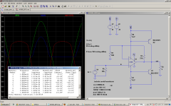
0.082389% 100W 4ohm LM ALONE
0.011403% 100W 4ohm 0,33
0.010787% 100W 4ohm 0,27
0.010884% 100W 4ohm 0,22
0.083993% 50W 8ohm LM ALONE
0.006442% 50W 8ohm 0,33
0.006143% 50W 8ohm 0,27
0.006422% 50W 8ohm 0,22
I would like made a TDA7293 amp with 2SC5200 / 2SA1943 pushpull (MJL on file but the 2SC/2SA are better on simulation)
Thanks to "dr frost dk" for giving us the idea.
It seems that this is a good amp but I prefer a diagram like this Attached File and many OPA application note
http://cds.linear.com/docs/en/application-note/an87f.pdf page 58
http://www.analog.com/static/imported-files/application_notes/28080533AN106.pdf page 1
http://www.stanford.edu/class/ee122/Parts_Info/datasheets/op_amp_circuit collection_AN-31.pdf page 19
http://bec.physics.monash.edu.au/wiki/Main/SpinorCoilDriver
Unfortunately there is no TDA7293 model, so I used a LM3886.
If you have a good LM3886 model, can you send it to me?
0.082389% 100W 4ohm LM ALONE
0.011403% 100W 4ohm 0,33
0.010787% 100W 4ohm 0,27
0.010884% 100W 4ohm 0,22
0.083993% 50W 8ohm LM ALONE
0.006442% 50W 8ohm 0,33
0.006143% 50W 8ohm 0,27
0.006422% 50W 8ohm 0,22
Attachments
Last edited:

Is this method of obtaining extra output current better, or worse, than paralleling chipamps?
What are the advantages and what are the disadvantages?
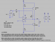
Remember to tap the output where it states "out" for the NFB resistor R4 (post1)
Post2 showing NFB R5 is correct.
What are the advantages and what are the disadvantages?
Remember to tap the output where it states "out" for the NFB resistor R4 (post1)
Post2 showing NFB R5 is correct.
Thank you for resistors, I would change
At the moment I do not know if one is better than the other.
I just know LINN audio abandoned the parallel implementation for the benefit of transistors
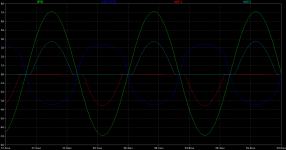
At first it is necessary to correctly simulate the diagram having reliable simulation model.
At the moment I do not know if one is better than the other.
I just know LINN audio abandoned the parallel implementation for the benefit of transistors
At first it is necessary to correctly simulate the diagram having reliable simulation model.
Last edited:
Hi all 🙂
I also think your idea could give better results than Dr Frost, because you won't have the VBE non-linearity I imagine there is in his output stage.
There's just a little thing I fear with your design: from my experience with a lot of TDA I burned (!), when the gap between the input stage (pins 7 & 8), and the power stage (pins 13 & 15) is not at least ~0.6V, the internal MOS transistors are not well polarized, and then the TDA dies (that's why Francis Ibre put a diode if I understand well)...
But in your design, I'm not sure you can ensure this constraint. Let me give an example...
If there is a 35V supply on VSS, you will certainly find something like 34.6V on VCC, but, unfortunately, the voltage drop you have in order to polarize the 2SA1947 will lead to a lower voltage on pin 13 (lets say 0.5V lower, so 34.5V). Am I wrong?
Maybe a solution to this would be to keep the initial diode system near the TDA, but inserting your transistor stage (R2 T3 R1 T2) in place of VSS and VEE on the right side of your schematics. I tried to draw my proposition in the following file.

There is also another detail I don't understand well: the package of the output transistors you choose (TO264 ?) is not really well suited to optimize power dissipation with a heatsink. My remark is maybe not relevant, as I didn't understand if your application is high power like Dr Frost, or audiophile like other suppliers you linked.
Hope it helps!
😉
Christophe
I also think your idea could give better results than Dr Frost, because you won't have the VBE non-linearity I imagine there is in his output stage.
There's just a little thing I fear with your design: from my experience with a lot of TDA I burned (!), when the gap between the input stage (pins 7 & 8), and the power stage (pins 13 & 15) is not at least ~0.6V, the internal MOS transistors are not well polarized, and then the TDA dies (that's why Francis Ibre put a diode if I understand well)...
But in your design, I'm not sure you can ensure this constraint. Let me give an example...
If there is a 35V supply on VSS, you will certainly find something like 34.6V on VCC, but, unfortunately, the voltage drop you have in order to polarize the 2SA1947 will lead to a lower voltage on pin 13 (lets say 0.5V lower, so 34.5V). Am I wrong?
Maybe a solution to this would be to keep the initial diode system near the TDA, but inserting your transistor stage (R2 T3 R1 T2) in place of VSS and VEE on the right side of your schematics. I tried to draw my proposition in the following file.
There is also another detail I don't understand well: the package of the output transistors you choose (TO264 ?) is not really well suited to optimize power dissipation with a heatsink. My remark is maybe not relevant, as I didn't understand if your application is high power like Dr Frost, or audiophile like other suppliers you linked.
Hope it helps!
😉
Christophe
Last edited:
Re-
After my post, I realized that at startup both 2SA and 2SC could be activated...
In my researches for an answer, I found the following link:
subwoofer amplifier 100W
I find the schematics a little... crowded but it's Worth studying 😉
see U
After my post, I realized that at startup both 2SA and 2SC could be activated...
In my researches for an answer, I found the following link:
subwoofer amplifier 100W
I find the schematics a little... crowded but it's Worth studying 😉
see U
- Status
- Not open for further replies.
- Home
- Amplifiers
- Chip Amps
- Gainclone LM3886/TDA7293 + 2SC2500 / 2SA1943 push