OK SMPS Gurus,
Here's what I cooked up over the weekend, and I need your input on it. Full-bridge, with P-Channels for the upper switches. I will post the schemo later today, but when you see it, you'll understand what I need to know:
If it is driven from any of the garden-variety PWM ICs (3525, 494, 33025, 1846, etc.), since both ends of the primary would be grounded (i.e. shorted) during the PWM's deadtime, how will this affect leakage inductance? I promise I will upload the schemo today.
Thanks in advance,
Steve
The MOSFETs should run hotter since they have to absorb the leakage inductance energy which is normally partially absorbed by snubber resisters. But the difference could be negligible depending on how your transformer is wound. Just a guess since factors like the MOSFET gate control signals' control over the switching times between the upper and lower MOSFETs would seem to factor in somewhat.
Sounds like a cool idea to try. I would hope it lowers EMI.
Sounds like a cool idea to try. I would hope it lowers EMI.
I forgot to mention that the MOSFETs in question are RFG50N06 and RFG60P05, so I would only be able to test this idea out on 12V or 24V systems.
I chose these two units because of their low Rds(on): 22mW for the N-CH, and 26mW for the P-CH.
Oh, if only someone could come up with a 500V P-CH with low Rds(on).
I chose these two units because of their low Rds(on): 22mW for the N-CH, and 26mW for the P-CH.
Oh, if only someone could come up with a 500V P-CH with low Rds(on).
i personally like the Schottky's.
as far as leakage inductance, will it matter that the opposing phase totem pole drive effectively grounds both sides during dead time?
would not the leakage inductance be nearly negated as a short or really low impedance on the primary?
it seems that it may be more ideal for the transformer to have no magnetic polarity or electrical charge.
however the initial current at turn on may be a bit lower since there should be no opposing polarity at all.
leakage inductance may be not matter since it is a period when no load is on the transformer.
what about the turn off current entering deadtime? could there b any secondary feedback?
mmmmmmmmmmmmmm😕 😕 😕 😕 😕 😕
I think I could substitute the 1N5819s with 1N4148s. Thoughts?
I think so too.
It appears to operate at very low slew rates, which I like in SMPS circuits. How does it do on the simulator?
Quote by Electrone: "I think so too.
It appears to operate at very low slew rates, which I like in SMPS circuits. How does it do on the simulator?"
Haven't done the simulation yet. I don't know if the schematic part of the free software from 4PCB.com has a simulator or not. If it does, I will try it.
As for the 1N4148's, I thought that since these N-channels might have rather large gate capacitances, perhaps a 1N4148 might not handle enough current, where the 1N5819 would. Either way, I will try this out on the simulator with both diodes. Fi there's no appreciable difference in performance, then I will go with the '4148's (cheaper and more plentiful).
I'd try the 11N4148 diodes and put them through tough testing just to see. Maybe you could temporarily quadruple the frequency of the gate drive to establish a good margin of reliability.
What do you want to drive with this circuit? The gate drive scheme won't work for anything but low frequency PWM, say below 1Khz.
Why full bridge for such a low voltage?
You get double on-resistance compared to push-pull N-channel with center-tapped transformer.
You have extra complexity, high impedance of gate driving circuit and 4 mosfets instead of two?
What about body diode of P-channel fets? it looks to me, that it is forward biased whenever N-channel turns on.
Please answer for I would like to understand your work.
Adam
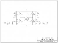
Edit: in schematic it is not clear where is source and where is drain of P-mosfets. I guess letters '1g' '2d' '3s' are correct and part symbol is not, right?
You get double on-resistance compared to push-pull N-channel with center-tapped transformer.
You have extra complexity, high impedance of gate driving circuit and 4 mosfets instead of two?
What about body diode of P-channel fets? it looks to me, that it is forward biased whenever N-channel turns on.
Please answer for I would like to understand your work.
Adam
Edit: in schematic it is not clear where is source and where is drain of P-mosfets. I guess letters '1g' '2d' '3s' are correct and part symbol is not, right?
Well,
Originally, this was part of a motor drive for a 24V PM motor. I was staring at it one day, and my mind began to wander (as it usually does.... ), and I got to thinkin': couldn't this thing be used in a half-bridge? Wandering still further, I completed the thought and saw the potential as a full-bridge.
In my earlier post, I said that we PWM'ed this at 70-100Hz, mainly because of the motor's moment of inertia. We had never really tested it past a few hundred Hz.
EVA- what do you see at the limiting factors? The Gate resistors? the large gate capacitance (4700pF)? Can I speed this up with a drive buffer? (Of course that would negate the P-Ch all together because the upper switch would need a floating drive to accomodate the drive buffer )
I am contemplating doing three half-bridge sections like this. If it doesn't work for SMPSs, then at least I will have a really robust low-voltage 3-F motor drive for brushless DC motors.
Originally, this was part of a motor drive for a 24V PM motor. I was staring at it one day, and my mind began to wander (as it usually does....
), and I got to thinkin': couldn't this thing be used in a half-bridge? Wandering still further, I completed the thought and saw the potential as a full-bridge. In my earlier post, I said that we PWM'ed this at 70-100Hz, mainly because of the motor's moment of inertia. We had never really tested it past a few hundred Hz.
EVA- what do you see at the limiting factors? The Gate resistors? the large gate capacitance (4700pF)? Can I speed this up with a drive buffer? (Of course that would negate the P-Ch all together because the upper switch would need a floating drive to accomodate the drive buffer
)I am contemplating doing three half-bridge sections like this. If it doesn't work for SMPSs, then at least I will have a really robust low-voltage 3-F motor drive for brushless DC motors.
darkfenriz said:Why full bridge for such a low voltage?
You get double on-resistance compared to push-pull N-channel with center-tapped transformer.
You have extra complexity, high impedance of gate driving circuit and 4 mosfets instead of two?
What about body diode of P-channel fets? it looks to me, that it is forward biased whenever N-channel turns on.
Please answer for I would like to understand your work.
Adam
Hi Adam,
Wel , because the only P-Channels I have seen for hi voltage are some ONSemi ones for 500V, but only 2A Drain current, with an Rds(on) of over 150mW. If I were going to drive anything over, say, 200W, I'd want a heftier device. The RFG60P05 had the largest drain current of any P-Ch I could find, that had at least a Vdss of 50V. So, in the absence of actually being able to implement this for off-line apps, I could verify its usefulness for low-voltage, high-current apps., like motor drive.
As fas as the P-Ch being forward biased at N-Ch turn-on, I don't think so, as the blocking action of the 2N2222 will bias it (the P-CH) at the rail (24V) effectively cutting it off. The arrangement of the biasing resistors as voltage dividers (as opposed to current dividers) insures that the MOSFETs will get a good "on" signal but not be overdriven to over 20V, if using a 24V bus. For 123V apps, this is not a concern, and the ratio of the biasing resistors can be . D 'ed to give a good signal to the gates.
As for gate drive complexity, it avoids the need for a floating drive for an upper-side N-CH, even at 24V, and it allows popular PWM ICs to directly drive it w/o need for a floating-gate driver IC or base-drive Xfmr.
Sorry if I talk in the abstract too much, but it has been a long time since I did the math on most of this ckt, and I had this sitting around for a while. My interest was renewed this last weekend, as I saw a potential app for it.
darkfenriz said:
Edit: in schematic it is not clear where is source and where is drain of P-mosfets. I guess letters '1g' '2d' '3s' are correct and part symbol is not, right?
You are correct. I only noticed this after checked it for netlist errors. The pinouts are correct, not the symbology.
I just realized something: I seem to remember a paragraph or two in the IR applicxation note in the IR2110 Floating Gate Driver IC: Using a P-ch for the hi-side would reduce the driver chip's power dissipation to zero. Before that, It stated that the chip could drive a P-Ch hi-side, but now, the HI(in) is tied to the LO(in). Anyway, I digress. I will attempt to fabricate this theis weekend, and report on its success/failure.
Continued input is still appreciated.
Has anyone ever tried this scheme?
Continued input is still appreciated.
Has anyone ever tried this scheme?
Gate drive is the limiting factor, with this arrangement switching events may take as long as 100us to complete (I haven't done the simulation, but I ended up with similar values for a 500Hz PWM motor driver in order to get smooth switching).
If you want to switch at several Khz, use all N-channel and floating driver ICs like IR2010 or HIP408x. Note that the main disadvantage of bootstrapped driver ICs is cost and that you can't keep the high side turned on forever, which may be a required feature when driving motors, lamps or a heaters, but not when driving a transformer. On the other hand, if you are going to drive a transformer at 24V, discard the full bridge in favour of a push-pull arrangement.
If you want to switch at several Khz, use all N-channel and floating driver ICs like IR2010 or HIP408x. Note that the main disadvantage of bootstrapped driver ICs is cost and that you can't keep the high side turned on forever, which may be a required feature when driving motors, lamps or a heaters, but not when driving a transformer. On the other hand, if you are going to drive a transformer at 24V, discard the full bridge in favour of a push-pull arrangement.
Darn! After hearing your comments, that's what I was afraid of.Quote by EVA: "On the other hand, if you are going to drive a transformer at 24V, discard the full bridge in favour of a push-pull arrangement."
I didn't really have an application (read: project) for this, but if it had worked, it would have given me an excuse to start yet another one. 😉
"So, how we doin'?"
"Well, looks like University of Illinois!"
(Motor control, here I come!!!) 😀
Thanks everyone for your input.
eva,
On the other hand, if you are going to drive a transformer at 24V, discard the full bridge in favour of a push-pull arrangement.
why not a full bridge at low voltage?
the advantages of flux walking would seem to help since the currents are higher...... or am I all wet??
Because of this:
http://www.irf.com/product-info/datasheets/data/irf2907z.pdf
With 75V devices like this one, whose typical Rds-on is .003 ohms and whose DC current rating comes from the own TO-220 package limits, who would want to switch high currents twice with floating gate drivers in a full bridge?
Paradoxically, I'm about to use these devices in a full bridge synchronous rectification stage, but it has to handle up to 52V (and up to 300A pulses, the diode arrays used in epilation lasers are very current hungry... 😎 )
- Status
- Not open for further replies.
- Home
- Amplifiers
- Power Supplies
- Full-Bridge Topology