Hey all,
I've been hemming and hawing on posting this as there's hundreds of phono pres here, but, I decided I'd go for it anyways. I'm absolutely brand new to PCB layout so hoping for some critique here.
The goal is quite simple, my last relationship left me with 4,000 records, but no turntable or pre-amp. I wanted to build a stage for MM, and I decided I wanted as much SMD as possible for practice. So in order of priority I wanted:
1) Something that works
2) A proven design
3) Mostly SMD as I want the practice
4) Reasonable layout practices
For the design I ended up picking Project 06 by Rod Elliott, and just tacked Project 87B on the end, which is the balance line transmitter.
For layout, I knew nothing, I had to go from vaguely recalling an intro to circuits class in college to actually laying out this thing. Major learning experience as I'm a CS, I understand C++ (which sadly doesn't mean Capacitors plus plus). I spent a week reading everything I could get my hands on, from Analog Devices Decoupling Capacitor papers to TI high speed layout techniques, and beyond to trolling forums.
Three things stood out to me as important:
1) Control impedance
2) Control loops
3) Try to limit input noise
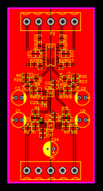
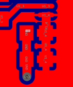
Nothing screams lower impedance to me than maximum width copper, so the top became V+ on left side and V- on right side. My understanding is with the bottom becoming GND that loops are minimal correct? To control noise I decoupled every power input with a .1uf and 10uf cap, with a 100uf power capacitor at the beginning to act as a reserve. Is this correct? Overkill? Not enough? From the 100uf power cap to the last IC is 1.5 inches, so under the 2 inches recommended by AD.
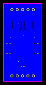
Finally, to control loops, I tried to not hop between layers with vias too much. Should I have put components on the bottom, or is keeping them all together and keeping a solid ground plane reasonable?
Overall how'd I do? Any major improvements or thoughts? I tried to take it logically, left input is on the left, right input is on the right, then carry it through, leaving room for power. Currently all parts are speced 0603 size, and the op amps I'm considering are opa1678/9. Not sure on power choice yet, still need to figure that out.
I've been hemming and hawing on posting this as there's hundreds of phono pres here, but, I decided I'd go for it anyways. I'm absolutely brand new to PCB layout so hoping for some critique here.
The goal is quite simple, my last relationship left me with 4,000 records, but no turntable or pre-amp. I wanted to build a stage for MM, and I decided I wanted as much SMD as possible for practice. So in order of priority I wanted:
1) Something that works
2) A proven design
3) Mostly SMD as I want the practice
4) Reasonable layout practices
For the design I ended up picking Project 06 by Rod Elliott, and just tacked Project 87B on the end, which is the balance line transmitter.
For layout, I knew nothing, I had to go from vaguely recalling an intro to circuits class in college to actually laying out this thing. Major learning experience as I'm a CS, I understand C++ (which sadly doesn't mean Capacitors plus plus). I spent a week reading everything I could get my hands on, from Analog Devices Decoupling Capacitor papers to TI high speed layout techniques, and beyond to trolling forums.
Three things stood out to me as important:
1) Control impedance
2) Control loops
3) Try to limit input noise
Nothing screams lower impedance to me than maximum width copper, so the top became V+ on left side and V- on right side. My understanding is with the bottom becoming GND that loops are minimal correct? To control noise I decoupled every power input with a .1uf and 10uf cap, with a 100uf power capacitor at the beginning to act as a reserve. Is this correct? Overkill? Not enough? From the 100uf power cap to the last IC is 1.5 inches, so under the 2 inches recommended by AD.
Finally, to control loops, I tried to not hop between layers with vias too much. Should I have put components on the bottom, or is keeping them all together and keeping a solid ground plane reasonable?
Overall how'd I do? Any major improvements or thoughts? I tried to take it logically, left input is on the left, right input is on the right, then carry it through, leaving room for power. Currently all parts are speced 0603 size, and the op amps I'm considering are opa1678/9. Not sure on power choice yet, still need to figure that out.
Attachments
Last edited:
I wanted to build a stage for MM, and I decided I wanted as much
SMD as possible for practice.
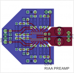
Looks pretty good, you should post the complete schematic for the pcb,
with the part numbers on it.
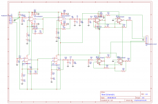
Oh right, I meant to do that. It's not laid out the cleanest as I was just copying.
The value of R9 is going to affect the T3 (R8*C4) value, because of no buffering.
Just use R29 alone, at least it causes <1% error. That will have better bass, too.
Last edited:
I was wondering about that. I inew they would be seen as in parallel, I just didn't know how it would affect things. If I just use R29, should I leave it as 100k?
The parallel value of R29 and R8 should be 750 so the T3 time constant is correct.
C4 * (R29//R8) = 75uS, and if C4 = 0.1uF, then R29//R8 = 750.
The R8 value could be increased with a small series resistor (~5R-6R), and then R29 could remain 100k and still have an accurate T3 value. Or just use R8=759R, and R29=63.4k. Then R8//R29=750.02, close enough.
C4 * (R29//R8) = 75uS, and if C4 = 0.1uF, then R29//R8 = 750.
The R8 value could be increased with a small series resistor (~5R-6R), and then R29 could remain 100k and still have an accurate T3 value. Or just use R8=759R, and R29=63.4k. Then R8//R29=750.02, close enough.
Last edited:
R1, R11, R8 and R13 are so high their thermal noise will dominate over the op-amp's noise.
Make sure to use good quality components: preferably thin-film resistors and definitely NO class 2 ceramics (X5R, X7R, Z5U, Y5V) as filtering capacitors, only class 1 (NP0, C0G) or film.
If this circuit has to go into an enclosure that also contains a power transformer, it can be useful to have a small-value resistor (100 ohm or so) in series with the grounded side of C1 and C6 that you short by connecting its upper side to ground at the input of the amplifier. That is, you could connect the ground of the input RCA connectors straight to the enclosure and have a shielded cable from the connectors to the input and the extra resistors. Just a trick to reduce the input to PCB and back to the ground side of the input loop area.
Why using ground planes for V+/V-?
I would prefer big copper plane to the decoupling caps before supply pins OPA?!
My 2 cents,
JP
I would prefer big copper plane to the decoupling caps before supply pins OPA?!
My 2 cents,
JP
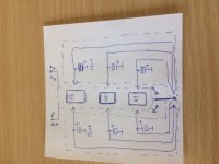
Dedicated connectors for signal and power.
Dedicated different ground planes for signal and power, following signals or power lines.
Star grounding?
My 2 + 2 cents,
JP
Dedicated different ground planes for signal and power, following signals or power lines.
Star grounding?
My 2 + 2 cents,
JP
The parallel value of R29 and R8 should be 750 so the T3 time constant is correct.
C4 * (R29//R8) = 75uS, and if C4 = 0.1uF, then R29//R8 = 750.
The R8 value could be increased with a small series resistor (~5R-6R), and then R29 could remain 100k and still have an accurate T3 value. Or just use R8=759R, and R29=63.4k. Then R8//R29=750.02, close enough.
I was planning to get a Signstek M4070, DE-5000, or Global Specialties LCR-58 and try to match components between channels as much as possible. Seems like it should be easy enough to run the math and try to find an R29//R8 = 750 pair.
Why using ground planes for V+/V-?
I would prefer big copper plane to the decoupling caps before supply pins OPA?!
My 2 cents,
JP
I was going off of this article which seemed to indicate that just connecting both pins to a power plane was better than explicitly routing power to caps then to IC. I've attached a closeup of one of the bypass cap layouts. My understanding is what I have is virtually identical to what's in the article. Any reason for doing it differently?
Edit to add: I'm using Easy Eda to create layout. I created a copper pour for V+/V-, it isn't part of the ground plane, unless I'm misunderstanding you.
Dedicated connectors for signal and power.
Dedicated different ground planes for signal and power, following signals or power lines.
Star grounding?
My 2 + 2 cents,
JP
I see what you're saying. I'm going to have to mull this over a bit more, I don't understand enough to see where/how much I'm compromising the system with my method vs yours.Something like this...
My 6 cents,
JP
Attachments
Last edited:
R1, R11, R8 and R13 are so high their thermal noise will dominate over the op-amp's noise.
Make sure to use good quality components: preferably thin-film resistors and definitely NO class 2 ceramics (X5R, X7R, Z5U, Y5V) as filtering capacitors, only class 1 (NP0, C0G) or film.
If this circuit has to go into an enclosure that also contains a power transformer, it can be useful to have a small-value resistor (100 ohm or so) in series with the grounded side of C1 and C6 that you short by connecting its upper side to ground at the input of the amplifier. That is, you could connect the ground of the input RCA connectors straight to the enclosure and have a shielded cable from the connectors to the input and the extra resistors. Just a trick to reduce the input to PCB and back to the ground side of the input loop area.
I'm leaning towards leaving power separate, make it modular so I can upgrade/replace as I learn more and improve things. I'll keep your recommendation in mind for the future though.
I'm having trouble finding 10uf caps that fit your recommendations, could you link some?
NP0 capacitors above 220 nF don't exist yet, as far as I know. In any case, the power supply decoupling capacitors can be class 2, just not the ones in the signal path (the RIAA correction filter capacitors C2, C4, C5, C7, C9 and C10 and the capacitors C1, C6, C3, C8).
For C1, C3, C6 and C8 normal aluminium (or aluminum since you're from the US) electrolytic capacitors should work OK, even though audiophiles generally don't like them. Bipolar electrolytic capacitors are better, but they're difficult to find as SMDs.
The really critical capacitors are those in the RIAA correction network, and their values are small enough to use NP0 / C0G.
Last edited:
A few comments that should improve the loop area and a better layout of the GND.
At the input, connect input GND, R12, C6, C9 and R30 together with a single connection to the power GND. See my simple layout where a separate power ground is used.
At the output, parallel traces from (U3) pin 1+7 to (P2) 1+2.
(U3) pin 5+R23 connecting together then connecting to GND.
At the input, connect input GND, R12, C6, C9 and R30 together with a single connection to the power GND. See my simple layout where a separate power ground is used.
At the output, parallel traces from (U3) pin 1+7 to (P2) 1+2.
(U3) pin 5+R23 connecting together then connecting to GND.
Attachments
The main pcb layout problem I found was with a power supply on the same pcb.
Mixing the smoothing caps charging impulses in with the audio ground is a recipe for disaster. However your not doing that here so it shouldn't be too dificult. I designed a USB mixer with power supply on the same pcb and didn't bother much with pcb layout.
I got 1VRMS of hum on the output with the input shorted !!
I would keep the input tracks as short as possible to keep noise down.
A ground plane is a great idea.
- Status
- Not open for further replies.
- Home
- Source & Line
- Analogue Source
- First PCB - SMD Phono pre