Hello. I have built a stereo channel ESP Project 3A amplifier using my own board layout, and have run into problems.
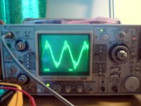
It sounds good on low levels, but I get some kind of distortion on higher volume levels. When I connected an oscilloscope and a sine wave, I saw that oscillations appeared on the top and bottom part of the sine wave after a certain volume level. Frequency of oscillation is near 1 MHz. A picture of the wave with oscillations is attached.
The same oscillation is also visible on the power supply from the capacitors, and there is no oscillation when the speakers is disconnected.
The speakers and everything else goes directly to a star ground.
Do anyone recognize this? It's hard to find the source of it because once it starts to oscillate it's everywhere in the amp.
My guess is a bad board layout. What's most important to think about when designing a good layout?
One other question, I have read that if only one power rail is applied, that voltage will appear on the output. But that holds true only for the negative rail in my amp, connecting only the positive rail will leave output at near 0V. Is this correct or wrong? (I've double checked the layout for errors, but still there could be something I missed)
Attachments
Do you have a picture of the setup and board layout? Where does speaker return go? Is there any local decoupling on board? Is the heatsink grounded and is the signal ground connected to chassis ground preferably with a loop breaker?
This sounds like something is wrong with either the output stage layout, its decoupling or possibly the speaker return wire.
"One other question, I have read that if only one power rail is applied, that voltage will appear on the output. But that holds true only for the negative rail in my amp, connecting only the positive rail will leave output at near 0V. Is this correct or wrong? (I've double checked the layout for errors, but still there could be something I missed)"
That is what should happen actually.
megajocke: Thanks, at least one thing that will stop bothering me. 🙂
Speaker return goes directly to a star ground on the capacitor board. Decoupling on the amp board is 100nF on + and -, and the heatsink is grounded. There is a 10R resistor between chassis and signal ground. Filter capacitors are 15 000µF / rail and channel.
Board layout This is the layout used. The ground plane is grounded at a single point, but after reading some posts here it seems a ground plane is no good idea? Also, input ground goes directly to the star ground and is not used on the board.
I'm working on a new layout that improves some things that I'm not happy with in the current one; like shorter output path, separate power/signal grounds etc.
The setup (Sorry for crappy quality) I know it looks like a mess. The output relay is connected to a DC protection circuit. The small wires goes to a clip detector and VU meter.
sakis: That's how it looks like when I measure it.
ok then ....
there is only two things i can say
one
never in my construction regarding amplifiers i ever used ground plane ..... destroys my ground rooting and star ground filosophy .....
also since i curently construct P3 not P3A ive noticed that this circuit ( probably others ) is kinda sensitive to ground rooting and signal return path ...... between 2 diferent pcb i ve constructed in diferent sizes it was a very audible diference ( i can post both pcb for experts to analyze since electrically speaking they are absolutely the same
two
it is very possible that ocilations comes up while all these secondary circuits are connected to the amplifier ( especially the way that they are connected )
try removing the protection and all the unrelated stuff to see for any changes
also inform us about overall performance and post some more wave forms at all conditions .....
all the best sakis
The P3A uses what is known as the CFP output, or the Sziklai Pair output (the NPN driver with PNP power transistor and vice versa). This particular combo is very sensitive to layout, and easy to make oscillate. Here's a few hints:
* Get rid of the ground plane. It will have a tendency to act like a big antenna and pick up crap, which will send the CFP output stage into oscillation.
* Shorten the power traces. Put the decoupling 100nF caps near the outputs. Better still, add 220-470uF decoupling caps, again near the output devices.
* Shorten the speaker output trace - better still dont have one, put the hole for the terminal right at the ends of the 0.33R resistors. You may want to try vertically mounting the resistors.
* Keep the feedback trace as short as possible.
* Why are you using such big parts for the Miller caps ? Silvered mica at a guess ? Don't bother on this design - polypropylene or polystyrene will be fine. You can even get away with good ceramics (like NPO types). Get em right near the transistor terminals.
* The 10R + 100nF that's on the output to ground is the Zobel network. You will want a 1W resistor here, and I usually use a Mylar capacitor. Personally I think Zobels are best placed at the speaker terminals.
* Put the BC546B that serves as the bias device (connected to the trimmer pot) near to one of the driver transistors. It's not strictly neccesary but it helps.
Return your speaker ground wire to the power supply's ground - not to the P3A board!
Oscillation at 1MHz is not really surprising, especially if you're using the MJL4281/4302 or similar parts.
P3A has no protection as such. The reason the amp will stay at zero when the -ve voltage is missing is because the current sink for the LTP doesn't start, and neither does the bootstrap current sink for the VAS.
Hi,
I would try eliminating the simple culprits first.
1) Your zobel network is connected to the input signal ground. This is very bad - naughty! At 1MHz the current through you zobel will become significant and will modulate the singal ground voltage.
Connect the zobel directly with its own wire to the star ground.
2) You speaker output connection is in the wrong place. You want to keep the high voltages and high currents of the output track and cable WELL AWAY from the input circuit. Naughty, naughty. The physical size of the 4.7uF i/p cap that crosses directly above the output trace will not be helping either.
I would perform a little surgery. Cut the output trace at the end by the 0R33 resistors. Scrape the resist away here and connect both the speaker wire and the zobel resistor directly here.
Get rid of the huge 4.7uF cap. Find a physically, much smaller input cap - like a tiny little polyproylene or polyester or a tantalum. Stick the cap right near the GND connector along with the i/p connector.
3) Your wiring is like spaghetti in the morning after a really wild night out . This creates a lot of stray magnetic and electric fields.
Is you star ground on that pcb board with the big caps?
Have 4 wires from the pcb board cable-tied closely together: pos, neg, zobel gnd, sig gnd. So you have two bunches, one for each amp.
Try each of these in turn until it stops oscillating. Then you will know what the main cause is. Then do the others too.
On you next board, don't bother with a ground plane - it causes more problems than it solves unless you a quite expert.
Hope you get it working. 🙂
I would try eliminating the simple culprits first.
1) Your zobel network is connected to the input signal ground. This is very bad - naughty!
At 1MHz the current through you zobel will become significant and will modulate the singal ground voltage.Connect the zobel directly with its own wire to the star ground.
2) You speaker output connection is in the wrong place. You want to keep the high voltages and high currents of the output track and cable WELL AWAY from the input circuit. Naughty, naughty.
The physical size of the 4.7uF i/p cap that crosses directly above the output trace will not be helping either.I would perform a little surgery. Cut the output trace at the end by the 0R33 resistors. Scrape the resist away here and connect both the speaker wire and the zobel resistor directly here.
Get rid of the huge 4.7uF cap. Find a physically, much smaller input cap - like a tiny little polyproylene or polyester or a tantalum. Stick the cap right near the GND connector along with the i/p connector.
3) Your wiring is like spaghetti in the morning after a really wild night out
. This creates a lot of stray magnetic and electric fields.Is you star ground on that pcb board with the big caps?
Have 4 wires from the pcb board cable-tied closely together: pos, neg, zobel gnd, sig gnd. So you have two bunches, one for each amp.
Try each of these in turn until it stops oscillating. Then you will know what the main cause is. Then do the others too.
On you next board, don't bother with a ground plane - it causes more problems than it solves unless you a quite expert.
Hope you get it working. 🙂
Thanks for the answers!
sakis: Didn't notice any improvement with the other stuff disconnected. But I found this: connecting 220µF to the rails helped some, oscillation vanished completely on the positive side of the wave and I think it decreased some on the negative (but was still there), so I guess a new layout is the only way to fix it.
jaycee: Thanks for the points!
The miller caps are polypropylene film foil, 1% 100pF. The P3a construction guide stated that close tolerance is advisable.
Connecting the zobel network to the speaker terminals would cause it to be disconnected from the amp during the power on delay, could this lead to problems?
traderbam: I had a bad feeling about having input and output so close, but thought of it first after the board was done. 🙂
I don't know about the input capacitor though, it's a polypropylene and recommended for audio usage so I'd rather keep it if I can.
The star ground is on the cap board, for both channels. I'll try to improve wiring in some way.
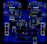
So I've worked on a new layout and is attached.
Some changes are:
* No ground plane (never again 😉)
* Output is taken between the two resistors, NFB point is taken exactly between those and shorted the trace.
* Moved decoupling capacitors closer to the output transistors and added the 220µF capacitors for each rail.
* Separate power and signal grounds.
* Might also consider moving the zobel-network to speaker terminals (but now I have separate grounds already).
Do you think this will work better?
sakis: Didn't notice any improvement with the other stuff disconnected. But I found this: connecting 220µF to the rails helped some, oscillation vanished completely on the positive side of the wave and I think it decreased some on the negative (but was still there), so I guess a new layout is the only way to fix it.
jaycee: Thanks for the points!
The miller caps are polypropylene film foil, 1% 100pF. The P3a construction guide stated that close tolerance is advisable.
Connecting the zobel network to the speaker terminals would cause it to be disconnected from the amp during the power on delay, could this lead to problems?
traderbam: I had a bad feeling about having input and output so close, but thought of it first after the board was done. 🙂
I don't know about the input capacitor though, it's a polypropylene and recommended for audio usage so I'd rather keep it if I can.
The star ground is on the cap board, for both channels. I'll try to improve wiring in some way.
So I've worked on a new layout and is attached.
Some changes are:
* No ground plane (never again 😉)
* Output is taken between the two resistors, NFB point is taken exactly between those and shorted the trace.
* Moved decoupling capacitors closer to the output transistors and added the 220µF capacitors for each rail.
* Separate power and signal grounds.
* Might also consider moving the zobel-network to speaker terminals (but now I have separate grounds already).
Do you think this will work better?
Attachments
That looks a lot better.
They are some big polypropylenes considering theyre 100pF. I usually use the Wima FKP2 series for this, and they have 5mm pitch.
The package for the 220pF capacitor in the input filter looks a bit small.. i'd make that a 5mm pitch part, a 5x7mm sized area.
They are some big polypropylenes considering theyre 100pF. I usually use the Wima FKP2 series for this, and they have 5mm pitch.
The package for the 220pF capacitor in the input filter looks a bit small.. i'd make that a 5mm pitch part, a 5x7mm sized area.
It looks much better but I'm worried about the loop formed around the card through transistors and decoupling. I'd try putting the dirty ground and decoupling/zobel between the output transistors if it's possible instead. I'd move the fuses and power input up closer to the transistors too and move down small signal stuff into the liberated space below. I think you can switch places of the two traces connecting driver and output on the right side and get much more space if they go straight instead of snake around each other. This way the right power rail can be brought around the transistor and meet decoupling in the middle. The power resistors will probably be at 90 degrees to what they are now for this to work.
Power supply, dirty ground and speaker wire should be twisted together or at least strapped together on their way back to the power supply where the speaker return is connected to power supply common.
A physically smaller input cap wouldn't hurt but you might be OK with the big one you have.
Power supply, dirty ground and speaker wire should be twisted together or at least strapped together on their way back to the power supply where the speaker return is connected to power supply common.
A physically smaller input cap wouldn't hurt but you might be OK with the big one you have.
I agree with jaycee and megajocke's comments.
I still think the 4.7uF i/p cap is unecessarily gross. It just makes a big antenna and is an exercise in "guilding the lilly". I have nothing against lillies. 🙂
You can get a small, 5mm pitch, radial cap that will be just as good and save you a bunch of board space. Tantalum are good, a film cap will be ok for this amp. There's a thread about this somewhere.
Hmm, looks like standard evil self-oscillating I'm used to see, that would destroy a fet(not sure about bjt's) pretty fast heh..
Personally I wouldnt use it if it couldnt drive a pretty large capacitor to ground so hmm A: Try to modify the circuit?(capacitor, output coil? or whatever)..or B:Trying to get it to work with different grounds, power suppy mods and so on..
hmm so far I couldnt get that type of output stage to work the way I wanted, but someday maybe.
Are thoose output stages tolerating capacitive loads better than a follower? I mean if it's oscillating a little now ,maybe it's gonna go nuts with another speaker or something..
I didn't put more effort in the design as I wanted to keep the board size and transistor positions so I took a chance and made that board (with only small modifications to make sure all parts would fit), and some initial tests indicated no more oscillations! 😀
I haven't tested with full power yet (will do when I get power resistors), and still haven't fixed wiring, but things looks promising so far.
But I wonder, with megajockes comment in regard, is there any good way to stress-test the amp for oscillations by using some typical difficult load and signals? (With the previous layout, I got remarkable more oscillations with the floor speakers than the small driver I'm using for testing)
I suggest that you change the 100nf caps for the outout pair to an axial type... then you could connect it, right at the pin, and still reach ground... A suitable roederstein will be maybe as big as a 1W resistor.
Nordic said:I suggest that you change the 100nf caps for the outout pair to an axial type... then you could connect it, right at the pin, and still reach ground... A suitable roederstein will be maybe as big as a 1W resistor.
thanks for the comment.
Do you mean move C12 and C13 to up near the output transistors, and connect to the pin on the transistor?
I'm not sure there would be any difference in the parasitic r-l-c between using etch on the pcb vs. the capacitor lead to make the connection. Any thoughts?
Aye, the reason I suggetsed the axial, was that it would limit the leadlenght, to reach your gound traces... could also be soldered under the board right to the relevant nodes.... I didn't see them in your last baord, but they were in the first ones...
Also try to star those many connections to the V+ and - rails, I think the best point is probably there where the fuse connects... you want mimimum common/shared traces with the large output traces...
Also try to star those many connections to the V+ and - rails, I think the best point is probably there where the fuse connects... you want mimimum common/shared traces with the large output traces...
mightydub, you have the VBE transistor on the main heatsink - dont do this in this design, the CFP output makes it unneccesary. It works better if it tracks the heat from one of the driver transistors.
Keep the 100nF decoupling caps near the transistors.
Keep the 100nF decoupling caps near the transistors.
Re: WAS THAT CORRECT ?????
i expressed my suprize about this 1mhz issue in the beging of the post and also i would like to express again a question about the procedures and the set up of this situation ....
i gave my advice about rerooting the pcb and get the ground plane dumped and so on and also i have seen others sharing the same opinions more or less with me ....
i also agree about the use of these big "antena caps " but then again the question is
WHAT IS EXACT SET UP FOR MEASURING OSCILATION IN THE AREA OF 1 MHZ ( I THINK I CAN CALL THAT RF) AND HOW CAN YOU GUARANTEE THAT THIS IS NOT "PICKED UP " BY YOUR SET UP .......
cause here we talk about rf ...it can be pickked up from any were and also i dlike to know is this oscilation what you ve seen creates any audible diference on how this device will sound ???
so is this really produced arround the amplifier or we are simply chasing a ghost ????
please place your opinion thank you
sakis said:1 MHZ ?????
i expressed my suprize about this 1mhz issue in the beging of the post and also i would like to express again a question about the procedures and the set up of this situation ....
i gave my advice about rerooting the pcb and get the ground plane dumped and so on and also i have seen others sharing the same opinions more or less with me ....
i also agree about the use of these big "antena caps " but then again the question is
WHAT IS EXACT SET UP FOR MEASURING OSCILATION IN THE AREA OF 1 MHZ ( I THINK I CAN CALL THAT RF) AND HOW CAN YOU GUARANTEE THAT THIS IS NOT "PICKED UP " BY YOUR SET UP .......
cause here we talk about rf ...it can be pickked up from any were and also i dlike to know is this oscilation what you ve seen creates any audible diference on how this device will sound ???
so is this really produced arround the amplifier or we are simply chasing a ghost ????
please place your opinion thank you
megajocke said:Do you have a picture of the setup and board layout? Where does speaker return go? Is there any local decoupling on board? Is the heatsink grounded and is the signal ground connected to chassis ground preferably with a loop breaker?
This sounds like something is wrong with either the output stage layout, its decoupling or possibly the speaker return wire.
"One other question, I have read that if only one power rail is applied, that voltage will appear on the output. But that holds true only for the negative rail in my amp, connecting only the positive rail will leave output at near 0V. Is this correct or wrong? (I've double checked the layout for errors, but still there could be something I missed)"
That is what should happen actually.
Tsuruya said:Thanks for the answers!
sakis: Didn't notice any improvement with the other stuff disconnected. But I found this: connecting 220µF to the rails helped some, oscillation vanished completely on the positive side of the wave and I think it decreased some on the negative (but was still there), so I guess a new layout is the only way to fix it.
jaycee: Thanks for the points!
The miller caps are polypropylene film foil, 1% 100pF. The P3a construction guide stated that close tolerance is advisable.
Connecting the zobel network to the speaker terminals would cause it to be disconnected from the amp during the power on delay, could this lead to problems?
traderbam: I had a bad feeling about having input and output so close, but thought of it first after the board was done. 🙂
I don't know about the input capacitor though, it's a polypropylene and recommended for audio usage so I'd rather keep it if I can.
The star ground is on the cap board, for both channels. I'll try to improve wiring in some way.
So I've worked on a new layout and is attached.
Some changes are:
* No ground plane (never again 😉)
* Output is taken between the two resistors, NFB point is taken exactly between those and shorted the trace.
* Moved decoupling capacitors closer to the output transistors and added the 220µF capacitors for each rail.
* Separate power and signal grounds.
* Might also consider moving the zobel-network to speaker terminals (but now I have separate grounds already).
Do you think this will work better?
Your "groundplane" is not connected to anytning.... so it is not a groundplane.
In order for the groundplane to work best, it must be unbroken, and thus single side PSBs are not really the best platform to use groundplanes on.
EDIT: A long time ago I made my own P3A layout - using a real goundplane - and had no problems with it.
\\\Jens
- Status
- Not open for further replies.
- Home
- Amplifiers
- Solid State
- ESP P3A oscillation problems