Hello, I have a Vox guitar amplifier with dsp frontend, that is, a modeling amp.
The dsp part of the amp is broken. There is no publicly available scheme for this amp, so I started to trace it's digital board and while doing it I realized that I don't understand what's going on in the ADC input circuit.
Could someone knowledgeable please explain what this circuit is?
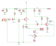
Below is the crude result of tracing, analog input part.
The markings on the sot-23 transistors:
Q1 - KY (possibly jfet KTK211, 2SK211 or 2SK881)
Q2, Q3 - MB (possibly bjt KTC2875)
The ADC in question is AKM AK5381 single ended 24Bit 96kHz ∆Σ ADC
What Q1 is doing? Some buffering, attenuation, protection - have no idea.
Q2, Q3 - the same. They are muting transistors btw, maybe that's some complicated muting circuit?
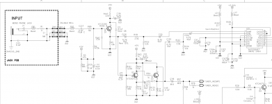
Also, I found a vaguely similar input arrangement in the Vox VT80+ schematics, but they used different parts there, please see the second pic.
The dsp part of the amp is broken. There is no publicly available scheme for this amp, so I started to trace it's digital board and while doing it I realized that I don't understand what's going on in the ADC input circuit.
Could someone knowledgeable please explain what this circuit is?
Below is the crude result of tracing, analog input part.
The markings on the sot-23 transistors:
Q1 - KY (possibly jfet KTK211, 2SK211 or 2SK881)
Q2, Q3 - MB (possibly bjt KTC2875)
The ADC in question is AKM AK5381 single ended 24Bit 96kHz ∆Σ ADC
What Q1 is doing? Some buffering, attenuation, protection - have no idea.
Q2, Q3 - the same. They are muting transistors btw, maybe that's some complicated muting circuit?
Also, I found a vaguely similar input arrangement in the Vox VT80+ schematics, but they used different parts there, please see the second pic.
Attachments
The fet is a buffer so the guitar sees a high input impedance. The other 2 transistors look like an inverter? Does the DAC have a balanced input?
Thank you for the clarification about the fet's function, this simplifies things a lot.
I would say no, but I didn't look closely to the DAC arrangement yet, the DAC is ak4384
https://www.akm.com/akm/en/file/datasheet/AK4384ET.pdf
Does the DAC have a balanced input?
I would say no, but I didn't look closely to the DAC arrangement yet, the DAC is ak4384
https://www.akm.com/akm/en/file/datasheet/AK4384ET.pdf
Looking at the 2nd schematic it appears Q1 is a buffer, Q2 is an amplifier, and Q3 is another buffer. The buffers feed the right and left inputs of the A/D. Q3 also drives the tuner, it looks like. Perhaps the reason for going in to both channels of the A/D at different gains is because guitars can have a very wide dynamic range. Perhaps. Or, maybe Q3 only routes into the A/D to drive a clip warning indicator. Something like that. Who knows.
Last edited:
Here is what I see, Q1 is an emitter follower, driving one of the ADC inputs and also driving Q2. Q2 is an inverter, which in turn drives another emitter follower Q3 to drive the opposite ADC input.
Your second drawing from some other model looks very much the same to me, other than it is drawn different.
The whole thing turns the single ended input into a balanced input for the ADC.
Your second drawing from some other model looks very much the same to me, other than it is drawn different.
The whole thing turns the single ended input into a balanced input for the ADC.
Thank you for the explanation, I was thinking that this may be a balanced input, but wasn't sure.
No, this maybe wrong as my only clues were the smd markings.
I only measured q1 with ohmmeter and it's supposed to be drain-source measures very similar to a jfet transistor.
I will double check the schematic.
In the first schematic are you sure that is a FET? The bias looks wrong for a N jfet.
No, this maybe wrong as my only clues were the smd markings.
I only measured q1 with ohmmeter and it's supposed to be drain-source measures very similar to a jfet transistor.
I will double check the schematic.
Q1 is biased fine, both versions. Gate is biased near half supply, source follows.
However the factory plan shows a BJT emitter follower. Bias can be essentially the same.
The "possible" plan: Q3 makes no sense at all.
The Factory plan: Q1 drives ADC's AINR pin at unity gain (nearly). Input overload is almost 2V peak.
Q2 Q3 provide gain of exactly 10, drive Tuner and ADC AINL pin. Input overload is near 0.2V peak.
You would think a "24 bit" ADC could resolve 144dB below 2V, or 0.1uV; but it won't. Input resolution is specced 102dB which works out to 15uV. Which is significantly more than a 12AX7 or a '741. With the 10X gain boost on the L input, the input resolution figures to be 1.5uV, fine for guitar.
(This smells like a minimum-cost design.)
The brains of the operation can take either L or R bits. If it is nowhere near overload, it would take bits from the 10X boosted path. When that gets near full scale, it can take bits from the non-boosted path. Result is nominally 20dB more dynamic range.
Last edited:
- Status
- Not open for further replies.
- Home
- Live Sound
- Instruments and Amps
- Enlighten me please - whats going on in this ADC input circuit?