Can a source component drive a small battery (perhaps voltage between +25mV and -25mV)?
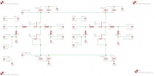
Does the following schematic work in practice?
It is an offset-trimmed DC coupled B1. It can be operated with simple (few number of parts, for example with LM7809 and LM7909) + and – power supplies. The difference between | + V_supply | and | - V_supply | should be stable, I think.

Does the following schematic work in practice?
It is an offset-trimmed DC coupled B1. It can be operated with simple (few number of parts, for example with LM7809 and LM7909) + and – power supplies. The difference between | + V_supply | and | - V_supply | should be stable, I think.
Last edited:
I think the above schematic fails unless the source component has output coupling capacitor. It can be corrected as follows, but it is not a DC B1.

That should work.
It's not DC B1 but you probably don't want that anyway? You don't want to amplify any DC from the source.
It's a B1 with no output offset.
It's not DC B1 but you probably don't want that anyway? You don't want to amplify any DC from the source.
It's a B1 with no output offset.
the active stage is a jFET acting as a source follower and it is loaded with a CCS using another jFET.
If the two jFETs are identical the Vgs of the source follower will be zero.
That means that the voltage on the gate is the same as the voltage on the source.
The source is connected to the load and thence to the signal ground.
This all results in the gate being at the same voltage as the signal ground.
You don't need a DC blocking capacitor on the input. The Input pin is referenced to signal ground and the follower is also referenced to the same signal ground.
You can run your buffer DC coupled throughout IF the two jFETs are identical.
But you have a bit of leeway. Simply select two (same model/type) jFETs with the same Idss.
If you want offset trimming look at Dennis Feucht.
This is what I expect from FET Audio.
2SK170BL match quad : HK$100 (about US$13 – 4 pcs). Idss 6.4 to 9mA only.
All matched within 0.2mA Idss @ 10Vdc. Note that the temperature at measurement is about 28 to 30 degC in Singapore.
0.2mA / 6.4mA = 3.125 %
2SK170BL match quad : HK$100 (about US$13 – 4 pcs). Idss 6.4 to 9mA only.
All matched within 0.2mA Idss @ 10Vdc. Note that the temperature at measurement is about 28 to 30 degC in Singapore.
0.2mA / 6.4mA = 3.125 %
Remeasure Idss.
select the top pair for one channel.
select the bottom pair for the other channel.
In each pair select the higher Idss for the upper device (source follower) and the slightly lower Idss for the lower device (CCS).
select the top pair for one channel.
select the bottom pair for the other channel.
In each pair select the higher Idss for the upper device (source follower) and the slightly lower Idss for the lower device (CCS).
- Status
- Not open for further replies.
- Home
- Amplifiers
- Pass Labs
- Does this DC B1 work?
