Does anybody know of actual measurements done which show the total inductance of a bypass capacitor with typical usage? By total inductance I mean effective loop inductance.
The reason I ask is I'm getting conflicting information, some saying a SMD 0603 close up to the pins has around 3nH, others saying different.
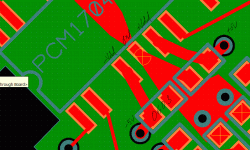
I used the estimator here on my layout, where a 0603 is 2mm from the IC pins (PCM1704), and got 20-30nH (!!!). How do you all estimate your trace inductances?
The reason I ask is I'm getting conflicting information, some saying a SMD 0603 close up to the pins has around 3nH, others saying different.
I used the estimator here on my layout, where a 0603 is 2mm from the IC pins (PCM1704), and got 20-30nH (!!!). How do you all estimate your trace inductances?
Also wanted to add that my layout is virtually identical to the recommended one in this app note and other places I've looked at.
If inductance really is 20-30nH, wouldn't that make the recommended pcm1704 4.7uf decap a poor choice for low jitter? It'd be around 1 ohm of impedance at 10mhz. That would lead to a lot of noise on the digital voltage reference and hence lots of jitter, regardless of how clean your clock was, isn't that correct?
If inductance really is 20-30nH, wouldn't that make the recommended pcm1704 4.7uf decap a poor choice for low jitter? It'd be around 1 ohm of impedance at 10mhz. That would lead to a lot of noise on the digital voltage reference and hence lots of jitter, regardless of how clean your clock was, isn't that correct?
trace inductance should be ~4..5nHI used the estimator here on my layout, where a 0603 is 2mm from the IC pins (PCM1704), and got 20-30nH (!!!)
Attachments
I know it should be, but I'd like to know what it actually is to make sure I'm not doing something wrong (and to optimise the decoupling). None of the formulas or calculators I've tried give reasonable results.
Can someone please take a look at this layout and tell if I'm doing something majorly wrong? (Layout is not finalised)
Can someone please take a look at this layout and tell if I'm doing something majorly wrong? (Layout is not finalised)
Attachments
Last edited:
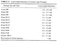
Ott (1988) says the typical minimum inductance is about 25nH. He says there's 5nH lead frame inductance per pin and about 3nH of trace between cap and pin.
If capacitor inductance is ~1nH for a 0603 that's right next to both supply pins, that still gives 1 (cap) + 3 (trace) + 10 (2*leads) + 3 (cap return trace) = 17nH. I'm looking for more references to confirm that number, but any advice from experienced members here would be appreciated.
If capacitor inductance is ~1nH for a 0603 that's right next to both supply pins, that still gives 1 (cap) + 3 (trace) + 10 (2*leads) + 3 (cap return trace) = 17nH. I'm looking for more references to confirm that number, but any advice from experienced members here would be appreciated.
Last edited:
I've looked into bypassing in ADC precision instrumentaiton applications - there are newer low inductance SMT "wide" termination caps and multi-terminal types for multi-MHz work - you're bascially screwed if you have to use through-hole parts
there is some info on what really happens in bypass applications and random paralleling of different caps can result in impedance peaks in the supply impedance
http://www.ultracad.com/articles/esrbcap.pdf shows the "anti-resonance" impedance peak you can get with the wrong choice of caps in parallel
http://www.pa.msu.edu/hep/d0/ftp/ru...nformation/xilinx_xapp623_decoupling_caps.pdf
also shows measured ps impedance peaking
the plots show ESR isn't always bad - lowers impecance peaking even if ultimate low Z is limited - sometimes introducing discrete R is a good idea
Last edited:
ouch, I'd have cleaned up spelling if diyaudio hadn't gone down
inductance you control can also be useful - pi filters with lossey SMT bead cores can be good at ps decoupling and limiting peaking
inductance you control can also be useful - pi filters with lossey SMT bead cores can be good at ps decoupling and limiting peaking
There's not much point simulating a decoupling network if you don't know the loop inductance though, at least approximately. Maybe Ott's numbers are so large because of thru-hole parts, but I haven't been able to find any other information on it yet. In any case, I doubt lead frame inductance has changed much. That gives us 8-10nH right off the bat, even without the traces, vias and capacitor(s). Maybe 5nH, thanks to smaller chips and having the supply pins near the die (as is on the PCM1704)? Questions, questions.
Last edited:
noCan someone please take a look at this layout and tell if I'm doing something majorly wrong?
oh yes yescan result in impedance peaks in the supply impedance
- Status
- Not open for further replies.
- Home
- Source & Line
- Digital Source
- Digital decoupling woes