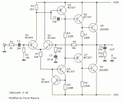
In the attached schematic,
1)How does the circuit, in its static(idle) state, ensure IcQ1=IcQ2? does it have something to do with the feedback resistor?
2)If R6 and R3 were calculated wrongly, could this cause DC offset at output of amplifier, even though Q1 & Q2 are matched?
3) Do R2 and R9 have to be matched to minimise offset? 😕
yes, if R3 and R6 are not properly proortional it will cause the differential input stage to go unbalance.
This should also cause an unbalance at the output thus creating DC offset.
This is my first impression looking at the circuit but I have never implemented it so maybe someone here will be able to give you a more solid answer.
Why are you using a single ended output stage. Do you have any benefit over the standard push-pull topology?
Another consideration aside looking at the schematic: the 47uF capacitor on the Feedback is used there to create an extra zero so that your overall DC gain drops down thus minimizing thermal issue and DC drifting at the output.
It is surely better than a servo control in certain aspects but its sound is going to be pretty bad and lack of live music sound.
It is surely better than a servo control in certain aspects but its sound is going to be pretty bad and lack of live music sound.
Another consideration aside looking at the schematic: the 47uF capacitor on the Feedback is used there to create an extra zero so that your overall DC gain drops down thus minimizing thermal issue and DC drifting at the output.
It is surely better than a servo control in certain aspects but its sound is going to be pretty bad and lack of live music.
I would stay aeay from it if I were you, the topology looks a bit old and over-compensated.
It is surely better than a servo control in certain aspects but its sound is going to be pretty bad and lack of live music.
I would stay aeay from it if I were you, the topology looks a bit old and over-compensated.
Look at any ss amplifier circuit from this 1970s-80s period. (Naim etc) They often have this same (R6) asymmetric resistance to balance collector currents because of loading by the the next amplifier transistor stage.
That was the plan. but it doesn't work properly and balance is not truly established so balanced Voltage Amplifier stages were developed to load both collectors and even more ambitious and complex stages have evolved to overcome these theoretical problems or just notional ideas of symmetry.
However, some of the most famous brands and some models still use this basic schema. and are still in demand. In which case, owners are probably not so convinced by modern technology as by a particular sound quality.
I would be surprised to find an old topology like this on a modern hi-end audio equipment.
Asymmetry of this design makes me wonder why anybody would still want to use it and sincerely don't see it matchin any hi0end standard of hi-resolution, natural sound and so on.
Asymmetry of this design makes me wonder why anybody would still want to use it and sincerely don't see it matchin any hi0end standard of hi-resolution, natural sound and so on.
Then consider yourself well surprised. - For just one manufacturer, Naim's circuits haven't changed since 1978!! Their prices at least are high enough to call "high-end"😀.
Regarding question #3: yes, assuming C1 is used, and/or the preceeding source has a series capacitor. This equalizes base voltages due to base currents.
Yes. E.g. If the current through Q1 is too high, that will cause Q3 to switch on harder, which will cause the amplifier's output voltage to rise. Since the output is connected to Q2's base via R9 (the feedback resistor), the voltage on Q2's base will also rise. Raising the voltage on Q2's base increases the current through Q2 and reduces the current through Q1, to correct the original imbalance.1)How does the circuit, in its static(idle) state, ensure IcQ1=IcQ2? does it have something to do with the feedback resistor?
Yes. The mechanism described above sets the current through Q1 to the amount required to correctly bias Q3 by the voltage across R6. If this is not half of the current through R3, then the currents through Q1 and Q2 will be different.2)If R6 and R3 were calculated wrongly, could this cause DC offset at output of amplifier, even though Q1 & Q2 are matched?
The resulting DC offset should be quite small. In the given circuit, if one transistor is conducting twice as much current as the other, the DC offset between their bases will only be about 25 mV, with a bit more at the amp's output due to the differences between the base currents of Q1 and Q2 causing different voltage drops across R2 and R9. If required, it's quite easy to change the circuit a bit to get zero DC offset at the output with mismatched currents in the input differential pair.
Interestingly, a lot of amps are deliberately designed to have mismatched currents in the input pair as this changes the distortion characteristics. OK, it causes a large increase in distortion, but the added distortion is mostly 2'nd harmonic. Not to get into a religious argument here, let's just say many people believe that amps with relatively higher amounts of low, even order distortion sound better.
Actually, now I look a bit closer, the circuit you posted looks like a good example of this.😀 I estimate about 1mA through R3 and about 0.3mA through R6 and Q1, so about 0.7mA through Q2, giving a 2 to 1 mismatch.
Yes, in theory. If the currents through Q1 and Q2 are the same and their current gains are the same, then their base currents will also be the same. In that case, you want R2 and R9 to be the same value so that the voltage drops across them are the same. If Q1 and Q2 aren't matched or their currents are different, then the whole thing's a bit of a crap-shoot anyway.3) Do R2 and R9 have to be matched to minimise offset?
For example, if Q1 and Q2 each conduct 0.5mA and have a current gain of 200, then the base currents will be 2.5uA and the voltage drops across R2 and R9 will both be 100mV. However if something's unbalanced then whatever the difference between the voltage drops across R2 and R9 is, will appear as DC offset at the output.
Hope some of that helps. 🙂
Attachments
Last edited:
That's the bit missed by most builders.then whatever the difference between the voltage drops across R2 and R9 is, will appear as DC offset at the output.
The difference between the base voltages plus the difference between the Rvdrop, is the output offset.
Imagine a perfectly matched pair of input devices where Vbe = Vbe' and hFE = hFE'
Further ensure that identical current Ie = Ie', and that Vce = Vce', then Pq = Pq' and the Tj = Tj'
Now we have two transistors at the same temperature with the same Ie and the same Vbe and the same Ib.
Set R2 = R9 and we end up with that earlier statement
Vbe + Vr2*Ib = Vbe' + Vr9*Ib'.
We have exactly Zero output offset.
Do not trim Re nor Re' to reduce the output offset.
Do not trim Ie nor Ie' to reduce the output offset.
Do not trim Vce nor Vce' to reduce output offset.
Find which error is creating the output offset. Trim output offset, without changing Pq and Pq'
That leaves you with either swapping input devices or trimming R2 and/or R9
Swapping devices is the best way to get the LTP working as an accurate (good) differential amplifier if all else has been properly set up to accurately match Left side with Right side of the LTP. The next best is to trim out a "small error" in Vbe by adjusting R2 and/or R9.
If the devices are thermally coupled and Pq is the same then the drift in output offset from cold to operating temperature will be very low. Unbalance the LTP in any way and you change the Tj side to side. That changes the "drift" in output offset.
In summary.
Do not unbalance the LTP away from being a good differential amplifier.
If Vbe @ Ie has a side to side error of 1mV then the output offset will have a error of 1mV IF if you keep the LTP in balance.
If you want to "tune" the sound of your amplifier to achieve a particular "niceness", then get the amp working properly first. Then investigate which method of unbalancing the accurate amplifier produces which kind of sound change. you can incorporate any number of deliberate inaccuracies to "tune" the amplifier sound. But, it won't be accurate.
Last edited:
- Status
- Not open for further replies.
- Home
- Amplifiers
- Solid State
- Differential pair questions