Hi all,
I wanted to use a Bourns 91 series dual conductive plastic pot in my project, but KiCAD does not include a compatible footprint, so I had to design my own. This is literally the first KiCAD footprint I have ever made.
Did I do a good job, what do you think? I tried to mimic the included footprints (e.g. for Alps RK163) as much as possible.
This is the original mechanical drawing from the datasheet:

And this is my footprint:

I used KiCAD's positioning tools to reference all pads and silkscreen to the origin point. The pads are 2mm in diameter with 0.85mm holes. My concern is that the holes might be a bit too tight to accommodate manufacturing tolerances...
I wanted to use a Bourns 91 series dual conductive plastic pot in my project, but KiCAD does not include a compatible footprint, so I had to design my own. This is literally the first KiCAD footprint I have ever made.
Did I do a good job, what do you think? I tried to mimic the included footprints (e.g. for Alps RK163) as much as possible.
This is the original mechanical drawing from the datasheet:
And this is my footprint:
I used KiCAD's positioning tools to reference all pads and silkscreen to the origin point. The pads are 2mm in diameter with 0.85mm holes. My concern is that the holes might be a bit too tight to accommodate manufacturing tolerances...
Attachments
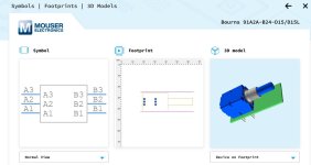
That Mouser info is awful.
Your finished hole size is too tight imo. It’s a square lead with max 0.81mm so what’s the hypotenuse? More than 0.85mm for sure , then add some extra hole clearance
Your finished hole size is too tight imo. It’s a square lead with max 0.81mm so what’s the hypotenuse? More than 0.85mm for sure , then add some extra hole clearance
Thanks, I didn't realize the leads were square. It seems the hole size should be 1.2mm. Sqrt(2*0.81^2) = 1.145
I do not recommend bourns pots because they usually come with a 1/4" = 6.3mm shaft -
useless with european 6.0mm knobs.
useless with european 6.0mm knobs.
I changed the hole size to 1.2mm and attached the footprint to the first post (in case anyone else finds it useful).
Last edited:
I didn't realize the leads were square. It seems the hole size should be 1.2mm. Sqrt(2*0.81^2) = 1.145
I have not seen many electronic component leads that are square, except for connectors, so I looked them up.
From the picture it looks like a cylindrical lead.
https://jp.rs-online.com/web/p/potentiometers/7899434?gb=s
https://jp.rs-online.com/web/p/potentiometers/6928682?gb=s
If they are plate-shaped, I think the thickness dimensions will also be specified on the drawings, as is the case with TDK.
Yep, it's an excellent pot and much better than the Alps RK27.Didn't know TKD, with conductive plastic they seem to be superior to ALPS.
That will have to wait until I have enough stuff in my shopping cart to qualify for free shipping 🙂It's always best to have one in hand when creating a footprint, that way you know for sure
Digikey's product thumbnails show round pins for Bourns series 91 pots.
I also designed a footprint for Bourns 91's using the DS dimensions as a starting point. BUT thru-hole dimensions shrink a bit due to the plateup so it's best to check the PCB manufacturer's specifications.....and add a bit more on top of that. I used 1mm holes and 2mm pads and that worked out OK. It's a LOT less frustrating to find that you need to use a little more solder, compared to not being able to install the pot.....
I also designed a footprint for Bourns 91's using the DS dimensions as a starting point. BUT thru-hole dimensions shrink a bit due to the plateup so it's best to check the PCB manufacturer's specifications.....and add a bit more on top of that. I used 1mm holes and 2mm pads and that worked out OK. It's a LOT less frustrating to find that you need to use a little more solder, compared to not being able to install the pot.....
- Home
- Design & Build
- Electronic Design
- Did I do a good job with this footprint?
