Hi everyone,
I'm trying to fix the second channel of this power amp I have. It's a Carvin DCA-800. A very nice amp indeed except it seems to be less than stable, probably due to the fact that the circuit boards are falling apart even though its only about 22 years old (same as me!). Anyway, its a quasi-complementary design and I have the schematic. It uses 6 MJ15003 for output. I keep testing it and blowing parts like capacitors and transistors ect. I don't believe that the output transistors are blowing (I hope not, but I'll check in a second).
Anyway, my question is, can I test the amplifier without the output power transistors in the circuit, or would this itself cause the amplifier to become unstable. I do have the schematic so I can answer questions.
Thanks,
Pete
If you put a 100W light bulb in series with the AC Main supply to the amp, you should be able to get time to do some electric and heat measuring before your components blow up 😉
Ok will do that.
I've made some progress so far. The boards have their own discrete voltage regulators on board, and I found out that the negative voltage reg wasn't working. The regs power the input stage (which is NE5532) and a pair of the pre-driver transistors (I could be wrong, the first set after the input stage...). With the power mosfets out of circuit I was able to get both regulators working.
I am now inputting a test tone to insure the input stage works. Can I test the VAS without connecting the output transistors (OPS)?
Pete
P.S. Gotta go buy a bulb!
Update:
I'm still working on the input stage. It seems to all be wired correctly and there doesn't seem to be any shorts or bad components. However, I've modeled the exact circuit from the schematic (to the best of my ability, perhaps a component is wrong) and the model doesn't seem to simulate correctly either. No wonder the circuit doesn't work.
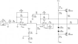
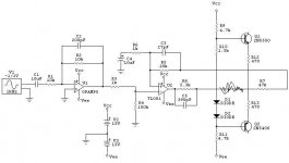
I've attached a picture of the input stage. Nothing dramatic here, just two stages of op amps. The input signal is fine up to the input of the second stage. I get a square wave output in simulation on the far side of R7. In the real circuit I get a DC offset of about 1/3rd Vee. I believe about -5V.
Is this diagram incorrect?
Pete
I'm still working on the input stage. It seems to all be wired correctly and there doesn't seem to be any shorts or bad components. However, I've modeled the exact circuit from the schematic (to the best of my ability, perhaps a component is wrong) and the model doesn't seem to simulate correctly either. No wonder the circuit doesn't work.
I've attached a picture of the input stage. Nothing dramatic here, just two stages of op amps. The input signal is fine up to the input of the second stage. I get a square wave output in simulation on the far side of R7. In the real circuit I get a DC offset of about 1/3rd Vee. I believe about -5V.
Is this diagram incorrect?
Pete
Attachments
Hello Peter. Well, amps can be tested without the output transistors so long as temporary jumpers are installed to make the feedback circuit think that they are there (minus their diode drop unless you substitute diodes to mimic the junction potentials of the internal base-emitter circuits). There probably are exceptions to this practice, but I have done it.
The above suggestion about operating the amp through a "short lamp" is well advised. Have success.
The above suggestion about operating the amp through a "short lamp" is well advised. Have success.
Thanks,
I'll try that. The original schematic that I was sent (very kindly by Carvin btw) is difficult to exactly what wires create a node and which wires cross each other. I'll play around in simulation for a bit to see if I can get it working, and I'll inspect the pcb to see if its supposed to touch but isn't.
Edit: It simulates correctly with an ideal op amp and gives a gain of about 20 (26dB). However, with a tl081 or tl071 etc it gives a square wave of 2V P-P with ringing. So perhaps the circuit is correct. What I'm basically really confused about is which nodes the connection between R7 and R8/C5 connects to.
Pete
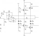
Here's a shot with some extra transistors. I can't remember what that's called (my Sloan book is at my friend's house!).
R7 is the global feedback resistor for the entire amplifier right? (I know thats obvious, but I'm learning...) I want to learn as much as I can about this particular amplifier because I will be designing a quasi-complementary amplifier within the next month (err, starting to design). Ok, so the output of the op amp stage must connect to R10 / D1. You mentioned the junction between D1 and D2 but it doesn't look like it in the diagram (they're much further down than where the lines cross). Although I bet it would work either way.
Pete
Attachments
- Status
- Not open for further replies.
- Home
- Amplifiers
- Solid State
- Debugging Quasi amp