Hello
I was thinking of assembling my next xover on a single side copper plated PCB like this one. So everything connected to the ground is soldered through a little hole to the copper plated part, the remaining connections wired p2p on the other side, and the components affixed with cable binders/hot glue.
What would be the advantages or downsides? Has anyone experiences. I was also considering to get oriented grain steel foils, which would then be used to wall the inductors, and that would also be connected to the ground plane.
Last edited:
As long as its mechanically sound should be ok.
There can be a lot of vibration in a speaker cabinet.
There can be a lot of vibration in a speaker cabinet.
Because current can not flow without voltage drop, any "ground" with current flowing in it is no longer equipotential. The 'correct' way to layout a crossover is to ensure that return currents from the different sections of the crossover and the different drivers do not share common current paths.
In a conventional layout the (-) from each driver should join directly to the (-) input terminal, and the shunt components of the crossover should solder to tracks that also go directly to the (-) input terminal or at least the track from the associated driver to the (-) input terminal. If you layout each section of the crossover so it could be separated into bi- or tri- wiring (i.e. separate (+) & (-) input connections for each driver's associated crossover section) you'll be most of the way to getting the optimum ground layout.
In a conventional layout the (-) from each driver should join directly to the (-) input terminal, and the shunt components of the crossover should solder to tracks that also go directly to the (-) input terminal or at least the track from the associated driver to the (-) input terminal. If you layout each section of the crossover so it could be separated into bi- or tri- wiring (i.e. separate (+) & (-) input connections for each driver's associated crossover section) you'll be most of the way to getting the optimum ground layout.
All that would happen is the voltages would add by a tiny amount dependent on copper pour resistance.
Correct, that is the problem to be avoided. Good design principles are good design principles.All that would happen is the voltages would add by a tiny amount dependent on copper pour resistance.
Ok thanks. I will make sure that all connections to ground will then be separate and join at the amp ground.
Take this or leave this, because I also use PCBs with substantial Earth planes, but thick earth planes produce measurable changes in inductance. This being a 1mH coil...
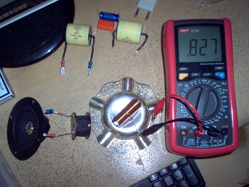
I would guess there might be crosstalk effects too. Only coils show changes. Capacitors and resistors seem immune. Thin foils like aluminium cooking foil produced little effect, it was the thick stuff that affected things. This is a silver ashtray for maximum conductivity.
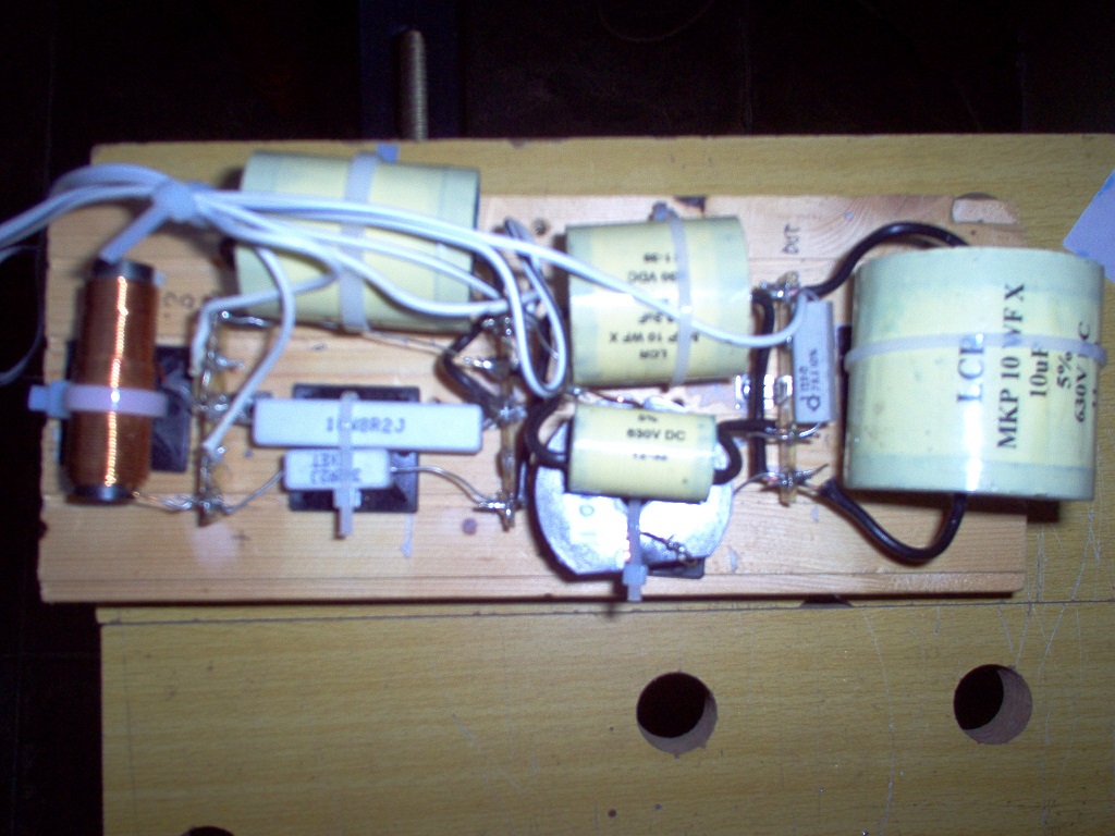
Thus my preferred layout is point to point:
I would guess there might be crosstalk effects too. Only coils show changes. Capacitors and resistors seem immune. Thin foils like aluminium cooking foil produced little effect, it was the thick stuff that affected things. This is a silver ashtray for maximum conductivity.
Thus my preferred layout is point to point:
But wouldnt they add at the common connection too ?
Well, then all connections to the common point should have either the same length or at least a very large section?!?
I mean, some minor potential differences are unavoidable. Maybe a copper “plate” may not be the worst solution?
Adding them together at the common input (-) point is the least worst solution, which will introduce the least intermodulation between driver voltage waveforms, and what is there then will be a function of the speaker cable alone, not the crossover.But wouldnt they add at the common connection too ?
How significant the intermodulation problems are in the proposed ground plane layout is indeterminate without knowing dozens more things about the drivers, the wiring, the thickness of the ground plane, the crossover topology, the position of components, etc, etc. But it is easy to eliminate intermodulation within the crossover circuit by using good layout, so why not do it? The same principles apply to ground layouts in preamplifier and power amplifier circuit layouts.
Last edited:
- Home
- Loudspeakers
- Multi-Way
- Crossover on a ground plane