What is your oppinion about common emitter / source amplifiers? I have designed a relatively simple circuit for a common source amplifier for home HiFi purpose. I like the almost rail to rail output voltage swing leading to lower rail voltages for a certain output power and less power dissipation.

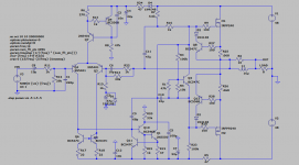
From left to right it consists of an input filter, a noninverting opamp circuit, a booster stage and a snubber circuit. The input filter blocks the dc and hf /rf. The opamp is used for the generation of the control currents of the booster stage. It has no output connection to the booster stage. The booster stage is controlled by the power rail currents of the opamp generating voltage drops across R4 and R5. It contains an adjustable current source (LM334, R8 is a trimmer) to set the quiescent current of the booster stage. The power MOSFETs M1, M2 are thermally stabilized by use of source resistors R9, R10 and large heat sinks (Rth = 10 K/W) in order to keep the channel temperatures between 50 and 100 °C.

The calculated FFT shows impressive THD of less than -60 dB. The quiescent current is set to 50 mA. Usually common emitter / source amplifiers tend to generate higher distortion levels compared to emitter / source follower amplifiers. For BJT booster stages I have also measured higher THD in the order of 1% at maximum Prms.
From left to right it consists of an input filter, a noninverting opamp circuit, a booster stage and a snubber circuit. The input filter blocks the dc and hf /rf. The opamp is used for the generation of the control currents of the booster stage. It has no output connection to the booster stage. The booster stage is controlled by the power rail currents of the opamp generating voltage drops across R4 and R5. It contains an adjustable current source (LM334, R8 is a trimmer) to set the quiescent current of the booster stage. The power MOSFETs M1, M2 are thermally stabilized by use of source resistors R9, R10 and large heat sinks (Rth = 10 K/W) in order to keep the channel temperatures between 50 and 100 °C.
The calculated FFT shows impressive THD of less than -60 dB. The quiescent current is set to 50 mA. Usually common emitter / source amplifiers tend to generate higher distortion levels compared to emitter / source follower amplifiers. For BJT booster stages I have also measured higher THD in the order of 1% at maximum Prms.
Last edited:
How about all discrete rail to rail. Like this Amplifier with 2 AA battery
I was looking into rail to rail topology. I haven’t found a good solution so far. Right now, if I need rail to rail, I would like to use good class D chip instead.
I was looking into rail to rail topology. I haven’t found a good solution so far. Right now, if I need rail to rail, I would like to use good class D chip instead.
Your design looks like a nice headphone amplifier. I think the design is rather complicated and the imput impedance is very low. I guess it is possibe to make such a discrete rail to rail amplifier with 6 transistors in total. I will try to make a design for it in order to see if it really works with +/- 1.2 V.
Last edited:
How about all discrete rail to rail. Like this Amplifier with 2 AA battery
Yes, it works with 6 transistors, look at this:
View attachment 966794
Last edited:
The calculated FFT shows impressive THD of less than -60 dB.
That's a pretty poor THD figure, certainly not impressive. A Blameless aims for 0.001% (-100dB) routinely.
The AD820 is very very poor at driving low impedance loads, giving it 47 ohm load will knacker its performance completely I think. Its open loop gain drops by a factor of 30 when load is reduced from 100k to 1k, so at 47 ohms it probably has a gain of a few 100.
BTW the topology is one way to avoid a standard VAS and thus the problem of unobtanium transistors. Done well its going to perform.
Last edited:
rail-rail
CE outputs have a couple issues including poor frequency/phase response and rail sticking. These issues can be minimized but EF outputs can also be "rail-rail" if you either use a boosted driver voltage or (partially) bootstrap the driver supply. For FETs, bootstrapping works very well because the gates are hi-Z. Then one wonders if the efficiency of class-AB amplifiers is an issue and those who need rail-rail output should consider class-D.
The attached MOS source follower amp is essentially rail-rail because it is boot-strapped in both directions.
Attachments
Your attachment seems not working.
You are right. Here is the circuit again for the +/- 1.2 V head phone common emitter amplifier.

That's a pretty poor THD figure, certainly not impressive. A Blameless aims for 0.001% (-100dB) routinely.
It depends what you want to get. In my opinion 0.1% THD is enough. Even 1% is mostly ok. Most of the commercial amplifiers are not better than that
The AD820 is very very poor at driving low impedance loads, giving it 47 ohm load will knacker its performance completely I think. Its open loop gain drops by a factor of 30 when load is reduced from 100k to 1k, so at 47 ohms it probably has a gain of a few 100.
This is not an issue because it doesn't need to drive the 47 Ohm load to a voltage higher that the input voltage. As I have mentioned, the total amplification is 48. Almost the total voltage amplification is done by the booster stage. The opamp is mainly there to provide the linearity in the feedback loop and to control the booster stage with its rail currents.
BTW the topology is one way to avoid a standard VAS and thus the problem of unobtanium transistors. Done well its going to perform.
What do you mean with "VAS"? I don't know all the abbreviations, I guess it is "voltage amplification stage". I am more in the field of controller technology not in audio.
Last edited:
...and those who need rail-rail output should consider class-D.
Class D is very complicated to DIY except you use pre-fabricated single chip class D amplifiers, but in this case you don't really know what these chips do.
The attached MOS source follower amp is essentially rail-rail because it is boot-strapped in both directions.
Yes, double boot-strapping is another option to get rail-to-rail output voltage swing for emitter / gate follower designs.
About your circuit in post#1: This is a MOS version of the classic rail driven boosted op-amp circuit. It is a fine DIY hack but not suitable for commercial production because the op-amp rail current is somewhat unpredictable. I would simply chose gate/base resistors instead of adding current with the LM337. I note that you did not use any local feedback to the op-amp output from the FET output. This may not be stable with some op-amps. It's important to realize how the op-amp output voltage swing effects the op-amp internal frequency compensation and therefor the feedback stability. If you short the op-amp output then there is no voltage swing which defeats the internal compensation. For amplifiers in this low voltage class, there are a b-zillion tiny chip amps, many of which feature very good sound ( and some that don't). The classic LM386 is very cheap, very simple, sounds pretty good...
You are right. Here is the circuit again for the +/- 1.2 V head phone common emitter amplifier.
View attachment 966927
Nice try.
The tricky part is the bias control, meanwhile maintains enough gain. You maybe already notice that.
I was not able to find a good solutions to that.
Ps: if you aim headphone amp, probably you could just use class A. Thus, you do not have to deal with the problem mentioned above.
Last edited:
Meanwhile I build up a test setup.


It is not so easy to set zero offset and a certain quiescent current but after a while I had it stable running with 10 mV offset and 5 mA quiescent current without drifting away. You have to work with relatively low quiescent currents. The offset and quiescent current settings are relatively sensitive to power supply voltage changes. So a low voltage adjustable current source at the emitters of the differential amplifier would be better if it is planned to operate it with two NiMH batteries.
I increased also the emitter resistors to 1 Ohm. I guess 4.7 Ohm or even 10 Ohm is better for more stability, but I had to limit it because of my headphone's 18 Ohm impedance. Because it is a mono amplifier I had to operate both channels at its output.
The sound was good, same like direct from the source. I have not yet measured it by oscilloscope, only with a true rms multimeter under audio control for distortion. At a symmetric power supply at 1.2 V I have 0.65 Vrms at 1 kHz. At 1.5 V I have 0.75 Vrms. So at 1.5 V an amplitude of 1 V can be achieved. Relating the input low pass filter R3, C2. I have removed C2, because there was no difference audible.
Last edited:
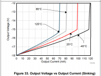
There is also another possibility of a +/- 1.2 V amplifier with +/- 1 V peek-to-peek output voltage swing by use of a low voltage opamp from Analog Devices.

- Home
- Amplifiers
- Solid State
- Common emitter / source amplifiers, rail to rail output voltage swing