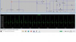
Greetings to everyone, I like to study amplifier curcuits but electronics is not my main activity. In this case I'm simulating a class H amplifier, I did simulations in Multisim and LTspice, I would like to know why the waveform in the differential pair transistor collector is deformed? Thanks in advance for the responses.
Attachments
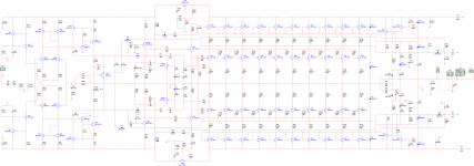
Do you have a Super Computer cuz there's no way I could simulate such 'complex' design with Multisim. Well, at least not in real time. I have tried couple of class H amps even those factory ones but to no avail. 
I understand, this circuit runs in multisim, but I find the deformed waves in the differential pairs collectors strange.

Greetings to everyone, I like to study amplifier curcuits but electronics is not my main activity. In this case I'm simulating a class H amplifier, I did simulations in Multisim and LTspice, I would like to know why the waveform in the differential pair transistor collector is deformed? Thanks in advance for the responses.
Have you checked the output stage isn't under-biased? That will throw all sorts of transients/oscillations around.
That “wave in the differential pair” is inside the feedback loop, after correction at the OUTPUT. Internal voltages/currents my may have all sorts of distortion.
^^^^ THAT.
* Input signal is clean by definition (specially in a Simulator 🙂 )
* Output signal is "as clean as possible" but of course there are lots of non linear stages inside that amp which WILL distort signal going through, to a larger or lesser degree.
* we have HEAVY negative feedback there, correcting errors.
* how does it know error and how does it try to correct it?
It compares input and output signal and extracts the difference,that´s why it´s called differential pair.
* how does it extract the difference? : by adding input and output signal out of phase.
When you do that, you are substracting one from the other.
* IF both signals are exact same (zero distortion) the substraction result is zero.
As in 1-1=zero, 397-397=zero, etc.
But they are not .... because circuit elements, as good as they may be, are more or less non linear, so difference will not be zero.
That difference is called error signal, will be wild looking (think of it as an extract of all errors present) and will be weird by definition.
* to boot, you are checking a voltage there, BUT:
a) you are checking a BE junction, a diode, a non linear element by definition.
b) that transistor is (more or less linearly) driven by current (bipolar transistor) which your
Simulator does not show and will be quite more linear, if not perfect of course, but you are watching a current signal driving a diode, no way you will see a linear (undistorted) signal there.
* test it yourself: drive a forward biased diode with a *current* sinewave and look at waveform.
* but output signal looks good!
Yes, error correction works. 🙂
NFB was a GREAT invention by Harold Black in 1927, the basic concept existing in a "mechanical" form for centuries and in living beings for some Million years , think temperature, blood sugar, etc. regulation.
It even applies in Economy (supply-demand price adjustment), etc.
Have you checked the output stage isn't under-biased? That will throw all sorts of transients/oscillations around.
I'm not sure about the translation, if the bias current is ok.
That “wave in the differential pair” is inside the feedback loop, after correction at the OUTPUT. Internal voltages/currents my may have all sorts of distortion.
I noticed that the wave varies according to the input signal strength and also when I changed the current source circuit of the differential pair.
^^^^ THAT.
* Input signal is clean by definition (specially in a Simulator 🙂 )
* Output signal is "as clean as possible" but of course there are lots of non linear stages inside that amp which WILL distort signal going through, to a larger or lesser degree.
* we have HEAVY negative feedback there, correcting errors.
* how does it know error and how does it try to correct it?
It compares input and output signal and extracts the difference,that´s why it´s called differential pair.
* how does it extract the difference? : by adding input and output signal out of phase.
When you do that, you are substracting one from the other.
* IF both signals are exact same (zero distortion) the substraction result is zero.
As in 1-1=zero, 397-397=zero, etc.
But they are not .... because circuit elements, as good as they may be, are more or less non linear, so difference will not be zero.
That difference is called error signal, will be wild looking (think of it as an extract of all errors present) and will be weird by definition.
* to boot, you are checking a voltage there, BUT:
a) you are checking a BE junction, a diode, a non linear element by definition.
b) that transistor is (more or less linearly) driven by current (bipolar transistor) which your
Simulator does not show and will be quite more linear, if not perfect of course, but you are watching a current signal driving a diode, no way you will see a linear (undistorted) signal there.
* test it yourself: drive a forward biased diode with a *current* sinewave and look at waveform.
* but output signal looks good!
Yes, error correction works. 🙂
NFB was a GREAT invention by Harold Black in 1927, the basic concept existing in a "mechanical" form for centuries and in living beings for some Million years , think temperature, blood sugar, etc. regulation.
It even applies in Economy (supply-demand price adjustment), etc.
Thanks JMFahey, what was strange to me was that when simulating a single differential pair amplifier, the sine signal was acceptable. So the deformed sinusoidal signal at this point is not worth worrying as the signal is ok at the output of the circuit?
The feedback tries to force the OUTPUT signal to be linear. Internal signals are what they are, in order to make that happen. If your output stage is distorting, then it’s drive signal is also distorted, in such a way as to cancel it (as much as possible, depending on the amount of available feedback).
If you simulate a differential pair on its own, connected to nothing or with a resistive load, signal will be quite clean, specially visually (you might measure a small distortion, say 1%), it is just a special case of a simple transistor gain stage.Thanks JMFahey, what was strange to me was that when simulating a single differential pair amplifier, the sine signal was acceptable
You are not using NFB and even less trying to correct "somebody else´s sins" which is what wgsky mentions.
In fact, output signal is ok because of this error correcting circuit.So the deformed sinusoidal signal at this point is not worth worrying as the signal is ok at the output of the circuit?
I understand, the information provided by you and JMFahey was very enlightening. I already follow your posts in other topics. Very grateful for solving this doubt.The feedback tries to force the OUTPUT signal to be linear. Internal signals are what they are, in order to make that happen. If your output stage is distorting, then it’s drive signal is also distorted, in such a way as to cancel it (as much as possible, depending on the amount of available feedback).
If you simulate a differential pair on its own, connected to nothing or with a resistive load, signal will be quite clean, specially visually (you might measure a small distortion, say 1%), it is just a special case of a simple transistor gain stage.
You are not using NFB and even less trying to correct "somebody else´s sins" which is what wgsky mentions.
In fact, output signal is ok because of this error correcting circuit.
Very grateful for the help JMFahey. as I mentioned, I already follow your posts and wgsky's posts in other forum threads, they are very useful to clarify doubts. Very grateful for solving this doubt.
The bias current is what flows through the output devices with zero input - it needs to be non-zero to allow for smoother transition on the cross-over between positive and negative output currents.I'm not sure about the translation, if the bias current is ok.
With under-biasing the output stage briefly goes to zero current at the cross over, destabilizing the amplifier very briefly, which can cause glitches round the feedback loop, or even short bursts of MHz oscillations.
- Home
- Amplifiers
- Solid State
- Class H amplifier, waveform in differential pair transistor collector