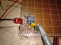
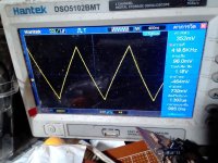
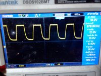
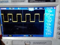
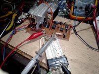
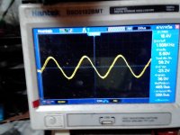
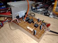
this circuit use ne555 gen tri-angle 400khz
Attachments
-
 265904681_1251691361976209_1477927957990063552_n.jpg155 KB · Views: 186
 -
 265962973_454835422662670_6025741732574330449_n.jpg117.3 KB · Views: 205
 -
 266335540_4611927992225419_990061036339089222_n.jpg89.4 KB · Views: 216
 -
 266289362_1112510956174077_4185127080228636291_n.jpg97.7 KB · Views: 190
 -
 266389611_509791093474257_7104265762823534453_n.jpg95.9 KB · Views: 168
 -
 265771180_622866262292429_4181169005048205786_n.jpg152.8 KB · Views: 161
 -
 266347422_690463855652685_6407712116307720166_n.jpg90.5 KB · Views: 162
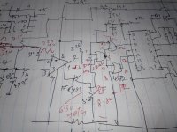
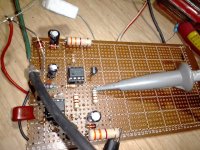
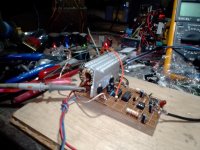
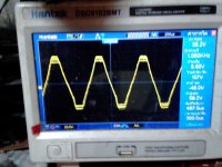
part 2 insert ic cd4070 separate phase sent forir2110
Attachments
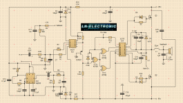

part3 insert ic ir2110 half bridgr dri and mosfet irf640
Attachments

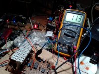
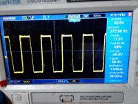
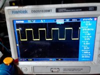
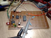
part4 test power at load 4 ohm vcc+-55v
Attachments

Surachit/Foodland Strikes Again.
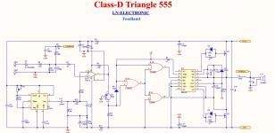
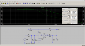
First off your circuits are inconsistent. Component identifiers differ across circuit diagrams as do some component values. Presumably you are doing this to hide your secret sauce of which there is none. You are really just wasting other people's time. At a minimum the timing capacitor for the 555 should be 470p to give you your 1.2V peak to peak triangle wave. That particular waveform is critical to distortion and yours is miserable given it is based on an RC network. Your power circuit gain is 120V/1.2V or 100, (peak to peak rail)/(peak to peak triangle). With a feedback factor of 50, 100K/2K, your loop gain, DC, is a whole 2, 6dB. This is why you can, almost, get away with post filter feedback which might make you claim to be a master but it is not worth having. Look at the crossover distortion for your 1KHz input. It results from dead time and you have no loop gain to deal with it. The circuit, as is typical with all the rubbish you produce, is still marginally stable despite your efforts to wob*. This is why your circuits infest forums elsewhere with some, paid?, posters making happy clappy wild claims of success whilst the rest complain about bin fires. Your amplifiers are an insult to the music you play on them and a plague on those who try to implement your continual fail.
Go Away.
*To Wob: Change random components for other random components until it seems to work.
Attachments
Last edited:
- Home
- Amplifiers
- Class D
- class d tri angle 555 step by step by foodland