Whilst my Class D amplifier is for low frequency RF usage on 136kHz it shares much with Class D audio amps, so i hope someone can put me straight on a few things please?
I have a push pull PA using 2 paralleled FET's per side. After a few mods lost me many FET's i am running just one FET per side to save money 😉 Whilst it was semi reliable with an inverting TC4426 driver IC with dual outputs it seems to have become very UNreliable since changing to a higher power TC4451 inverting IC driver. These have single outputs, so I am using two of them. My main question is do I need some dead time with this topology or not? It appears neither of these drivers have inbuilt dead time circuitry.
The amp is now run from either a single 52V at umpteen amps SMPS from a computer server, or for high power, two of them in series. A linear power supply makes no difference to FET failure rates, even at a miserable 30V!
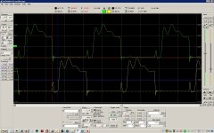
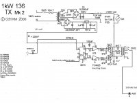
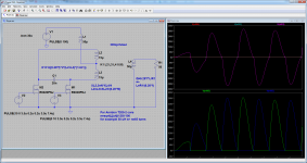
I attach spec sheets for the two different driver IC's, the gate and drain waveforms, and the basic 9abridged) schematic for the amp. In have added 470nF caps between the driver chip and the flip flop to stop DC driving, and Schottzy diodes across the 6R8 resistors, to no avail.
Secondly, pre the low pass output filter, I see these gate and drain wave forms and comments are very welcome.
Thanks.
I have a push pull PA using 2 paralleled FET's per side. After a few mods lost me many FET's i am running just one FET per side to save money 😉 Whilst it was semi reliable with an inverting TC4426 driver IC with dual outputs it seems to have become very UNreliable since changing to a higher power TC4451 inverting IC driver. These have single outputs, so I am using two of them. My main question is do I need some dead time with this topology or not? It appears neither of these drivers have inbuilt dead time circuitry.
The amp is now run from either a single 52V at umpteen amps SMPS from a computer server, or for high power, two of them in series. A linear power supply makes no difference to FET failure rates, even at a miserable 30V!
I attach spec sheets for the two different driver IC's, the gate and drain waveforms, and the basic 9abridged) schematic for the amp. In have added 470nF caps between the driver chip and the flip flop to stop DC driving, and Schottzy diodes across the 6R8 resistors, to no avail.
Secondly, pre the low pass output filter, I see these gate and drain wave forms and comments are very welcome.
Thanks.
Attachments
In this topology you must have negative or zero dead time. This seems OK.
But in this topology you should tune the output to resonance:
https://en.wikipedia.org/wiki/Royer_oscillator#/media/File:Royer_oscillator.gif
Capacitor must be a polipropilene type!
The second problematic thing is that you should control the inrush current, otherwise at startup voltage may go to about twice of the steady state.
I would say this is much more of a power supply than an amplifier, but I don't mind if it is here.
Drain waveforms should be like this:
https://videoflier.com/web/jesseg/2013-08-02_17-57-04_298-resized.jpg
https://videoflier.com/web/jesseg/2013-08-02_17-57-04_298-resized.jpg
Dead time must be avoided in this topology.
Number 1 problem here is the lack of tuning. Number of turns and capacitance must be set first. According to the load impedance. Which is unknown...
Number 1 problem here is the lack of tuning. Number of turns and capacitance must be set first. According to the load impedance. Which is unknown...
Whilst my Class D amplifier is for low frequency RF usage on 136kHz it shares much with Class D audio amps, so i hope someone can put me straight on a few things please?
I have a push pull PA using 2 paralleled FET's per side. After a few mods lost me many FET's i am running just one FET per side to save money 😉 Whilst it was semi reliable with an inverting TC4426 driver IC with dual outputs it seems to have become very UNreliable since changing to a higher power TC4451 inverting IC driver. These have single outputs, so I am using two of them. My main question is do I need some dead time with this topology or not? It appears neither of these drivers have inbuilt dead time circuitry.
The amp is now run from either a single 52V at umpteen amps SMPS from a computer server, or for high power, two of them in series. A linear power supply makes no difference to FET failure rates, even at a miserable 30V!
I attach spec sheets for the two different driver IC's, the gate and drain waveforms, and the basic 9abridged) schematic for the amp. In have added 470nF caps between the driver chip and the flip flop to stop DC driving, and Schottzy diodes across the 6R8 resistors, to no avail.
Secondly, pre the low pass output filter, I see these gate and drain wave forms and comments are very welcome.
Thanks.
What do you mean "pre low pass output filter"? I can't see any low pass output filter.
Gates can be protected by zener diodes, but if you do the tuning and layout right they are unneccessary.
added 470nF caps between the driver chip and the flip flop to stop DC driving
It doesn't help, since there is no DC current on input of drivers. If you really want to switch the MOSFETs off this way when no signal, then apply pull-up resistors on driver input! 10nF and 22k may be OK. But correct protection via set and reset pins of 4013 is much better.
Schottzy diodes across the 6R8 resistors, to no avail.
What is the direction of the schottky diodes, and what "to no avail." means?
Last edited:
Thanks for the answers so far, the load to be matched is 50 Ohms, I have been told the Zobel network might be better replaced by a series cap and resistor to ground on each side of the primary, deleting the 4n7caps.
Drain waveform deteriorates immediately if I start to remove the half inch ferrite rod that is the core for CH1. I may experiment with a toroidal cored choke, Good idea?
Drain waveform deteriorates immediately if I start to remove the half inch ferrite rod that is the core for CH1. I may experiment with a toroidal cored choke, Good idea?
What do you mean "pre low pass output filter"? I can't see any low pass output filter.
Gates can be protected by zener diodes, but if you do the tuning and layout right they are unneccessary.
It doesn't help, since there is no DC current on input of drivers. If you really want to switch the MOSFETs off this way when no signal, then apply pull-up resistors on driver input! 10nF and 22k may be OK. But correct protection via set and reset pins of 4013 is much better.
What is the direction of the schottky diodes, and what "to no avail." means?
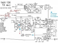
Hi Pafi, thanks for some great help. The schematic I showed is abbreviated (cut down, not showing everything). I attach the original schematic, which has been slightly altered over the years. After the output transformer there is a low pass filter network, then co-ax to outside the house, to a toroidal wound impedance matching transformer, then a huge loading coil to the antenna.
OK, I understand re the gates and Zeners, thank you.
The 470nF caps I have put in line from the flip flop to the driver IC's was to stop any chance of a rogue signal holding one FET on and shorting. It's used by many amp designers for LF RF work. My blown FET problem didn't improve since I fitted them though 🙁
I put fast diodes, Schottky ones, across the 6R8 resistors, with cathodes towards the flip flop 4013. I was told they would add some dead time, but I am learning we do not need, nor do we want any dead time. "To no avail" means they did no good, still FEt's fail.
Whether this is important or not I do not know, but 99% of the time only one FET fails. Due to cost of changing them I am running only one FET per side, and the one that always fails, unless both do, is the Q3 / Q4. I do not know why this should be...
I appreciate your patient help, thanks Pafi.
Attachments
Thanks for the answers so far, the load to be matched is 50 Ohms, I have been told the Zobel network might be better replaced by a series cap and resistor to ground on each side of the primary, deleting the 4n7caps.
Drain waveform deteriorates immediately if I start to remove the half inch ferrite rod that is the core for CH1. I may experiment with a toroidal cored choke, Good idea?
I hope you misunderstood the first advice. Zobel network is basically not needed at all. Pure capacitance is needed strongly, and would be better to connect 1 between drains, but the connection like it is now is also usable, however not economic.
You need similar or more inductance here as in the output transformer. A good toroidal (as T200-2) is better than a ferrite rod, however it depends on number of turns and geometry (of the rod).
But the first you should do is tuning it to resonance!!!
There are more capacitance and inductance combinations can be selected for the same frequency, the difference between them is the quality factor.
For example for Q=1 you need about 50 uH on secondary. This is not the best for harmonic suppression, but still usable, and much better than the currently built.
I attached a proposed power section dimensioning.
Attachments
Hi Chris,
So were those drain waveforms measured while the low pass filter was not connected?
If this is the case, then you'd better retest it with LPF and load.
If not, then the waveform tells that transformer inductance is too low, coupling is too weak, or both.
When damage happens? (During what operation?)
Hi again Pafi! Please remember I am a novice with electronics, learning as I go along. I need pretty simple explanations, my maths is not very good! Many thanks for your optimised circuits. I will try and rebuild the transformer using that data. Today I have tried a few experiments using what I have to hand here. Firstly I wound a different choke (CH1). I used a t157-26 core and used 25 turns of #14 enamelled wire. I see FAR less RF on the supply side now. Everyone who builds similar amps is absolutely sure that I must use a cap (470nF seems the common choice) between the driver and the 6R8 resistor, as the 4013, with no input signal, can hold a FET conducting. I have a no signal safety circuit, but a cap, I am told, makes double sure a FET can't short.
When I add a 470nF cap I also need to add a Schottky diode to ground from the junction of the cap and the 6R8 resistor, to restore full drive to the FET. Without it I see a much reduced gate waveform, and s reduced power output. I assume the FET's are not being fully turned on without the diode?
I had poor bypassing on the power pins of the two driver chips. I added 2uF ceramic caps right at the pins to the ground plane.
I was still losing FET's though.
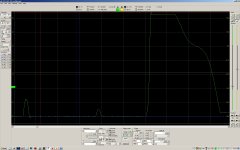
I then put my scope on single trigger mode and looked at the drain voltages. When a TX session started all seemed OK, *BUT* when a TX finished I often see a spike, up to 720V in some cases, often two spikes about 52uS apart. I will attach a capture below. You ask when damage happens. 90% of the time it's happening when a TX finishes and drive is removed. 12V remains on all the time, 50V remains on all the time. Just the 272kHz drive is removed., It's then a FET often fails. Gate to drain short, sometimes drain to source, sometimes all three shorted together. This spike is well over the max voltage the FET is designed for...
BE AWARE the scope capture used a X20 attenuator as the spike was going out of range of my USB scope, so the Y axis figures need to be multiplied by 20 X. The horizontal cursors show how big it is, the figure at the top of 37V is really 740V !!
You ask about LPF. All scope captures are with the LPF after the transformer, and either into a 50 Ohm dummy load, or a well matched antenna. I am going to see if the spike is there into a dummy load, or just the antenna.
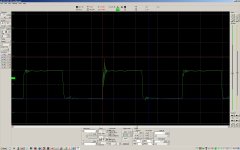
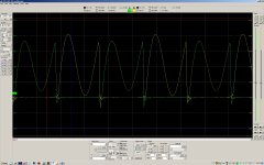
Finally I tried this new low pass filter set up I built. To me a low pass filter is a low pass filter, changing design to this 5 element one should, if anything, improve things. This new filter, the design linked below, appears to have caused the drain wave forms to be TOTALLY different from the original one with only two toroids. Can a LPF change the drain wave forms Pafi?
Does anything I mention make sense to you, I am just telling you everything I think might have some meaning to the problem, sorry if some of it is obvious. Thanks for your patient help!
When I add a 470nF cap I also need to add a Schottky diode to ground from the junction of the cap and the 6R8 resistor, to restore full drive to the FET. Without it I see a much reduced gate waveform, and s reduced power output. I assume the FET's are not being fully turned on without the diode?
I had poor bypassing on the power pins of the two driver chips. I added 2uF ceramic caps right at the pins to the ground plane.
I was still losing FET's though.
I then put my scope on single trigger mode and looked at the drain voltages. When a TX session started all seemed OK, *BUT* when a TX finished I often see a spike, up to 720V in some cases, often two spikes about 52uS apart. I will attach a capture below. You ask when damage happens. 90% of the time it's happening when a TX finishes and drive is removed. 12V remains on all the time, 50V remains on all the time. Just the 272kHz drive is removed., It's then a FET often fails. Gate to drain short, sometimes drain to source, sometimes all three shorted together. This spike is well over the max voltage the FET is designed for...
BE AWARE the scope capture used a X20 attenuator as the spike was going out of range of my USB scope, so the Y axis figures need to be multiplied by 20 X. The horizontal cursors show how big it is, the figure at the top of 37V is really 740V !!
You ask about LPF. All scope captures are with the LPF after the transformer, and either into a 50 Ohm dummy load, or a well matched antenna. I am going to see if the spike is there into a dummy load, or just the antenna.
Finally I tried this new low pass filter set up I built. To me a low pass filter is a low pass filter, changing design to this 5 element one should, if anything, improve things. This new filter, the design linked below, appears to have caused the drain wave forms to be TOTALLY different from the original one with only two toroids. Can a LPF change the drain wave forms Pafi?
Does anything I mention make sense to you, I am just telling you everything I think might have some meaning to the problem, sorry if some of it is obvious. Thanks for your patient help!
Attachments
Hi again Pafi! Please remember I am a novice with electronics, learning as I go along. I need pretty simple explanations, my maths is not very good! Many thanks for your optimised circuits. I will try and rebuild the transformer using that data. Today I have tried a few experiments using what I have to hand here. Firstly I wound a different choke (CH1). I used a t157-26 core and used 25 turns of #14 enamelled wire.
Good, it must have much higher inductance, but haven't it become hot?
Never mind! The key element is the transformer, not the choke. What is it like now?
I see FAR less RF on the supply side now. Everyone who builds similar amps is absolutely sure that I must use a cap (470nF seems the common choice) between the driver and the 6R8 resistor, as the 4013, with no input signal, can hold a FET conducting. I have a no signal safety circuit, but a cap, I am told, makes double sure a FET can't short.
Double sure means sure was not really sure. The basic circuit should be good.
You said before: "In have added 470nF caps between the driver chip and the flip flop to stop DC driving" It's not the same as "between the driver and the 6R8 resistor".
When I add a 470nF cap I also need to add a Schottky diode to ground from the junction of the cap and the 6R8 resistor, to restore full drive to the FET. Without it I see a much reduced gate waveform, and s reduced power output. I assume the FET's are not being fully turned on without the diode?
That is true. DC component is cancelled by cap, and restored by the schottky.
I had poor bypassing on the power pins of the two driver chips. I added 2uF ceramic caps right at the pins to the ground plane.
I was still losing FET's though.
I then put my scope on single trigger mode and looked at the drain voltages. When a TX session started all seemed OK, *BUT* when a TX finished I often see a spike, up to 720V in some cases, often two spikes about 52uS apart. I will attach a capture below. You ask when damage happens. 90% of the time it's happening when a TX finishes and drive is removed. 12V remains on all the time, 50V remains on all the time. Just the 272kHz drive is removed.,
This is important. In this moment you need to turn off both FETs. If I guess correctly IC3 is responsible for timeout protection, but maybe it works too slowly. Unfortunately I don't have time for analysing the whole circuit (what is only a part of the fully operating setup), but you could check if it works correctly or not.
What signal finishes TX session? What is red X?
It's then a FET often fails. Gate to drain short, sometimes drain to source, sometimes all three shorted together. This spike is well over the max voltage the FET is designed for...
BE AWARE the scope capture used a X20 attenuator as the spike was going out of range of my USB scope, so the Y axis figures need to be multiplied by 20 X. The horizontal cursors show how big it is, the figure at the top of 37V is really 740V !!
You ask about LPF. All scope captures are with the LPF after the transformer, and either into a 50 Ohm dummy load, or a well matched antenna. I am going to see if the spike is there into a dummy load, or just the antenna.
Finally I tried this new low pass filter set up I built. To me a low pass filter is a low pass filter, changing design to this 5 element one should, if anything, improve things. This new filter, the design linked below, appears to have caused the drain wave forms to be TOTALLY different from the original one with only two toroids. Can a LPF change the drain wave forms Pafi?
Yes, absolutely. Its input admittance (1/impedance) should have the same reactive part as the output of the oscillator, but with different polarity. The original is capacitive, yours is inductive, surely they can't work the same way. But neither of the waveforms are correct.
Still I don't know how to interprete your attached scope screens. You said all of them made with LPF. The very first one also? And which LPF of the 2 you shown?
Since LPF changes impedance seen by oscillator from pure 50 ohm to capacitively or inductively reactive, its internal reactances must be changed.
According to both scope measurements you need more drain capacitance, to make waveform similar to half sine. To be able to tell what capacitance is needed, you need to experiment, or to tell what is the output transformer looks like now (core and numbers of turns and physical arrangement, or measured inductances including leakage inductance).
But this is only the 0th step, probably you need to change control circuit also, to switch off FETs fast enough!
Overvoltage after turn-off is normal. The question is what current flows during this, and how long. 1 drain voltage alone, without knowing any of the inductances, and without knowing any other signal is not enough for any analysis. But if you think this was the problem (I'm not sure about it), then you can use DCR (Diode+Capacitor+Resistor) subber to eat it. C>20 nF.
LPF can start with C or L, neither one is more real LPF than the other. But your LPF seems to have more input impedance at 138 kHz than 50 ohm. I tell this because I simulated it together with my previous power stage, and I got lower antenne voltage, and higher drain voltage. Unfortunately I didn't have time to measure impedances. Maybe it's normal that near corner freq input and output impedance doesn't match, but then turns ratio of transformer must be modified (to higher).
What is the allowed harmonic content for your transmitter? Probably it's better to filter out some harmonics by tuned zeros (notch filter). Less inductors are needed.
What is the allowed harmonic content for your transmitter? Probably it's better to filter out some harmonics by tuned zeros (notch filter). Less inductors are needed.
dr om
Is this used for CW (telegraphy) ? In this case don't ever think of keying the clock to the D - flip-flop as this will definitely lead to FET failure. The clock must always be present in order to prevent the "one FET on for longer time" situation.
Keying must be done via logic NAND gates after the D-FF. It would be elegant to key via the D input of the second half of the D-FF, which by itself is running from the same clock as the first one, in order to guarantee that the FETs are always on for a full 180 degrees.
73
Charles (from HB9)
Edit: And yes Pafi's version of placing the tank circuit capacitor is more elegant than two caps to ground.
- Status
- Not open for further replies.
- Home
- Amplifiers
- Class D
- Class D push pull. Dead time required??