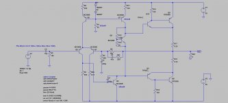
Hi guys,
Currently i'm designing an AB amplifier just for fun, i build an amplifier before based on STK 084 module (over 20 years ago) . Well now im building a new design which i simulated in multisim. I read the book of amplifier design of malestrom. But i'm having some difficulties. When i simulate my circuit i get a strange ripple on the positive half wave of the audio signal. I have no clue what the cause is. Is there anyone who knows what causes the ripple? Underneath the schematic and simulation output. I really would appreciate help!! I already made the PCB boards so i hope this can be solved by adjusting component values.


Kind regards,
Geert
Currently i'm designing an AB amplifier just for fun, i build an amplifier before based on STK 084 module (over 20 years ago) . Well now im building a new design which i simulated in multisim. I read the book of amplifier design of malestrom. But i'm having some difficulties. When i simulate my circuit i get a strange ripple on the positive half wave of the audio signal. I have no clue what the cause is. Is there anyone who knows what causes the ripple? Underneath the schematic and simulation output. I really would appreciate help!! I already made the PCB boards so i hope this can be solved by adjusting component values.
Kind regards,
Geert
One thing I note is the two CFP outputs see different source impedance at RF - there's normally a capacitor across
the Vbe multiplier to prevent this mismatch.
But basically oscillation like this is due to inadequate compensation, generally - what's the square-wave response?
Can you plot the open-loop gain/phase?
the Vbe multiplier to prevent this mismatch.
But basically oscillation like this is due to inadequate compensation, generally - what's the square-wave response?
Can you plot the open-loop gain/phase?
Yes, Vbe multiplier to by bypassed by 100nF-1uF. R8 is useless, it makes only optical balancing of the input diff. R7 value to be tuned to get current balance of both halves of the input pair. I can see no output RC Zobel, try something like 10R+22nF.
Hi.
I also simulated the circuit in LTspice.
With your values I get the oscillation too. Also, there is no reasonable bias in the output stage, and the square wave response contains oscillations and overshoots.
I changed some values in the simulation:
# Bias of about 60mA in the output stage.
# LTP: the same current flows in both tails.
# Rectangle response is now quite usable.
You should consider the power dissipation of some components, I wrote them alongside in my simulation. The BC556/546 transistors in VAS and CCS would get quiet hot, they wouldn't last long.

Attachments
Also don't use BC546 for the VAS (Q3) at 35V, It will overheat. Likewise it's opposite BC556.
If you're going for budget or easily obtainable, MJE340/350 work well enough as VAS devices.
If you're going for budget or easily obtainable, MJE340/350 work well enough as VAS devices.
Thank you for the useful tips. I added a 100 nF capacitor across the VBE multiplier and the oscilations were gone! The Constant current sources deliver 3 mA in the input stage, and 6 mA in the VAS i can't imagine that overheating will be problematic with this low currents. Ofcourse i will consider to use other transistors as suggested as long as the footprints are the same.
@ Mark tillotson how do i plot the open loop gain? Do you mean the Gain of the VAS? I dont understand what you exactly mean.
@ catD bias current 60 mA is the quiescent current in the driver transistors i suppose? How do i open the .asc file? is it with LTspice software? is it freeware?
Thanks for the help guys!!
Underneath the quiescent current. about 44 mA. CCS delivering 3 resp. 6 mA.

Beneath input and output signal

@ Mark tillotson how do i plot the open loop gain? Do you mean the Gain of the VAS? I dont understand what you exactly mean.
@ catD bias current 60 mA is the quiescent current in the driver transistors i suppose? How do i open the .asc file? is it with LTspice software? is it freeware?
Thanks for the help guys!!
Underneath the quiescent current. about 44 mA. CCS delivering 3 resp. 6 mA.
Beneath input and output signal
You have a CFP / Sziklai output circuit using slow driver transistors, which may be unstable. Stability requires one stage to be much slower than the rest, and a TIP41/42 is not much faster than a 3055/2955. I recommend faster driver transistors and a Zobel network. TIP41/42 are 4mHz 7A transistors and you need a 2A 50MHz transistor for drivers. Bypassing the VBE network helps by lowering the impedance to the driver base, but it is still marginal.
Basic phase margin measurement is usually a stimulus in series with the feedback and plot the ratio of the voltages on each side of that stimulus, ie output/ input (feedback), usually from 1 Hz to 100MHz. A more complicated probe is called the Tian probe, but it is almost the same and much more complicated. Search for it in DIYA. Examples are included with LTC Spice.
BTW+/-35V is pushing 3055/2955 transistors to their limit. Use a lower supply voltage (~+/-25V) or larger output transistors (~2sc5200/2sa1943).
- Home
- Amplifiers
- Solid State
- Class AB amplifier issues. Simulation multisim