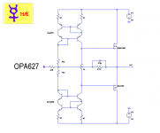
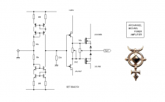
The feature of this design:
is not to have the input stage
assigned to an operational amplifier BB OPA627
the gain is reduced very
all to the benefit of sound zero feedback
then the feedback actually becomes
a DC servo

changes are welcome on graphics 🙂
is not to have the input stage
assigned to an operational amplifier BB OPA627
the gain is reduced very
all to the benefit of sound zero feedback
then the feedback actually becomes
a DC servo
changes are welcome on graphics 🙂
Attachments
Stee,
A very truly good design indeed. I have made quite a number of variations of this design since 1982 and am quite pleased with the results of each.
Best Regards,
Rich
A very truly good design indeed. I have made quite a number of variations of this design since 1982 and am quite pleased with the results of each.
Best Regards,
Rich
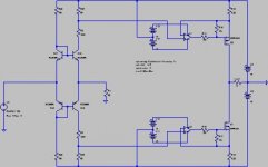
Stee, maybe you posted the wrong picture.
In your diagram, the input stage is an OPA627, but you say it is not.😕The feature of this design:
is not to have the input stage
assigned to an operational amplifier BB OPA627
There is feedback through the 8.1K resistor, but you say there is zero feedback.😕the gain is reduced very
all to the benefit of sound zero feedback
Where is the DC servo?😕then the feedback actually becomes
a DC servo
Re: maybe you posted the wrong picture
Godfrey,
I read Stee's post as an opener to an idea for those of us so inclined to build upon together.
I read his post as - the circuit is not to have the input stage
assigned to an operational amplifier BB OPA627 like he has depicted.
The gain of the circuit is quite low thus the connections provided by the 8.1K ohm resistor is to instead represent the fuction as would a servo loop.
Hope this helps.
Best Regards,
Rich
Fair enough, Rich
I see a couple of problems with Stee's circuit. Firstly, the open loop gain is badly defined and the open loop bandwidth is severely limited. If the amp is to be used without feedback, it would be useful to add resistors from each MOSFET gate to ground, to set the gain and improve the frequency response.
Secondly, the output stage bias current is strongly dependent on the supply voltage. That can be fixed by cascoding the 10K resistors at some stable lower voltage.
Other issues to be addressed are: getting rid of the feedback, eliminating the need for an opamp buffer or other input stage, and implementing a DC servo.
~~~~~~~~~~~~~~~~~~~~~~~~~~~~~~~~~~~
I think the circuit below is a step in the right direction.
Input impedance is 5K and voltage gain is about 10. It includes a crude but effective passive DC servo with a time constant of about 1 second, using properly biased electrolytic capacitors.
VR1 allows adjustment of the output stage bias current. Note that if the trimmer dies open circuit, the output devices are switched off rather than being fried.
VR2 allows adjustment of DC offset. The bypass resistors ensure that offset stays reasonable even if that trimmer dies.
I've simplified the current mirrors to save space on the drawing, but in fact they need to be improved as even the ones Stee used will introduce a significant amount of distortion.
If the mirrors could be given some current gain, then R10 and R17 could be reduced to improve bandwidth and/or the input impedance or voltage gain could be increased.
Cheers - Godfrey
p.s. @ Steve Eddy & co: By "feedback", I mean global feedback. I am aware that source followers, current mirrors etc use feedback.😛
Attachments
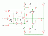
Sorry everyone for the small graphic on my first post.
Here is a higher resolution of the idea I first posted to compliment Stee's last night
Just a note on it. Although it would somewhat function as is, it would require a current source to drive it.
Again, just an idea I threw together at the moment.
As is, it is non-switching.
Best Regards,
Rich
Here is a higher resolution of the idea I first posted to compliment Stee's last night
Just a note on it. Although it would somewhat function as is, it would require a current source to drive it.
Again, just an idea I threw together at the moment.
As is, it is non-switching.
Best Regards,
Rich
Attachments
Both seem to me two interesting developments
Godfrey, however, seems to better suited to the DIY
because the concept of a minimal
is more appealing to a natural sound
As the valve without feedback
I would say that is excellent
Godfrey, however, seems to better suited to the DIY
because the concept of a minimal
is more appealing to a natural sound
As the valve without feedback
I would say that is excellent
What I like about this kind if circuit is the way the output current is shared between the two output devices - quite similar to a valve amp.Here is a higher resolution of the idea I first posted to compliment Stee's last night
Just a note on it. Although it would somewhat function as is, it would require a current source to drive it.
In the given circuit, there will be distortion from the input stage, though. With voltage drive, there is distortion due to Vbe non-linearity of Q18 and Q15. With current drive, there is distortion due to non-linearity and mismatching of the current gain of Q18 and Q15.
This can be avoided by grounding the existing input, removing the 58 Ohm resistor, and applying current input at that point.
Thanks, Stee.Both seem to me two interesting developments
Stee,
Although my circuit lost your approval, for the benefit of the rest of our community that may be curious, I will impart some details of how it functions while keeping the narrative as simple as possible.
You are right that the circuit complexity is increased with the two flying bipolar supplies and the respective Mosfet drivers, although there are numerous honest advantages.
The circuit can be considered as two function blocks.
The first function block translates both quiescent current of the input circuit mutually with its dynamic current directly proportional to the input signal, to establish and govern the bias current magnitude of the Mosfet power transistors of the output stage.
The second function block tracks and maintains each of the Mosfet power transistors bias magnitude independently within its respective linear operating region relative to the dynamics of the load and functional characteristics of the Mosfet.
Thus as for the extra supplies, one ±10VDC bi-polar supply for driver U1 is referenced to +40VDC (flying) (which then measures +50 and +30 VDC referenced to ground) while the other ±10VDC bi-polar supply for U2 is referenced to –40VDC (flying) (which then measures –50 and –30 VDC referenced to ground). The reason to utilize ±10VDC driver supplies is to protect the Mosfet gates from over-potential. Furthermore any sag in the main supply is tracked by the flying supplies while not affecting Mosfet drive.
Each Mosfet is driven in a very tightly controlled fashion. As frequency increases, Mosfet gate current increases. Although if the output would be composed of bipolar junction transistors (BJT’s), their equivalent operational base currents would need to be about 1 amp a piece. Power Mosfets have a much lower input current requirement than bipolar junction transistors although input capacitance becomes quite significant with increasing frequency, which increases the demand to properly drive it. Therefore the driver (which could even be any applicable op-amp given it can produce at least 10 ma output current) handles all that without any effect reflected to preceding circuitry.
The Mosfet power transistors are arranged common source, each source series connected through a source resistance to a respective power supply rail, wherein the drains are parallel combined at the output.
The steady-state supply current drawn by Q15 through Q18 sets a DC current across collector resistors R2 and R3, together with R27 & R30, directly biasing U1 & U2 to produce, track and maintain (servo if you wish) each current across the respective 0.22W Mosfet source resistors R18 & R19 to each be the same conducted by each respective Mosfet gate. In simple terms, the Mosfets bias’s are set by the steady-state supply current drawn by Q15 through Q18.
Each Mosfet driver drives the respective MOSFET gate to develop (force) a match between the 0.22Ω sense resistor drop and the VIN current command. Characteristic differences between N & P Mosfets become mostly eliminated.
In a nutshell, when a signal is applied to the input, the current across collector resistors R2 and R3, together with R27 & R30 becomes modulated precisely proportional to an exact replica of the signal combined with the bias current. Without the need for global feedback.
Godfrey, thank you for your compliment, you added very nice enhancements to Stee's idea.
Best Regards,
Rich
Last edited:
trust me, I'm a Designer 😛
I believe you are. You are quite resourceful. You have done many (new?) ideas that I haven't seen before. I cannot do something similar for sure. Coz I'm not a designer. But I can use designers ideas (JLH, Nelson Pass, You) and put them together to make a better sounding amp than yours

No offense. That's life. There are many others who don't know anything but selling other people's ideas and make money from it. Variety of skills. Which one is your favorite? 😀
So,
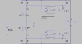
Jay and Stee let's say I'd like to get rid of the opamps managing Vout of the Vout balanced DAC in my old but trustworthy JVC XLZ574.
I'd like to go with FET output stage. Any advice?
TIA,
Stefano
Jay and Stee let's say I'd like to get rid of the opamps managing Vout of the Vout balanced DAC in my old but trustworthy JVC XLZ574.
I'd like to go with FET output stage. Any advice?
TIA,
Stefano
- Status
- Not open for further replies.
- Home
- Amplifiers
- Solid State
- CLASS A MOSFET OUTPUT STAGE