Hi everyone !
i wanted to make a PCB ESL for a long long time, its just gone be mid/treble panel with some features to segment it later on (so divided by 3 for instance)... but i had problems with the only PCB software i know EasyEda (perfect for electronics, not for other things you can do with pcb), all pcb software is based on a schematic. parts etc and then make a pcb. i myself work in sketchup... yes old... and crap. but thats what i would like to use or something similar . any one has an idea of a piece of software where you can draw you panel (mostly holes and dictate where copper is gone be and where is not, double sides or preferred even 4 layers to encapsule the copper)
i ca import a DXF into easyeda, and make all circles a cut trough thats one step... but i want the copper not extend to the edge of the holes... and i would like if possible the copper to be embedded in layer 2 or 3.. so no painting or whatever is required.
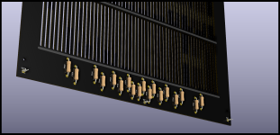
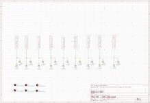
does anyone have a idea what works simple and i can upload to JLCpcb for instance ? image is of an imported DXF in easy eda. but i dont know where to start. i dont want just holes...(i want the copper to be slightly bigger hole so it wont arc etc , and i want to make segmented parts... but not to sure how , since the PCB programs are mostly based on the schematic. instead of just drawing 🙂)

i wanted to make a PCB ESL for a long long time, its just gone be mid/treble panel with some features to segment it later on (so divided by 3 for instance)... but i had problems with the only PCB software i know EasyEda (perfect for electronics, not for other things you can do with pcb), all pcb software is based on a schematic. parts etc and then make a pcb. i myself work in sketchup... yes old... and crap. but thats what i would like to use or something similar . any one has an idea of a piece of software where you can draw you panel (mostly holes and dictate where copper is gone be and where is not, double sides or preferred even 4 layers to encapsule the copper)
i ca import a DXF into easyeda, and make all circles a cut trough thats one step... but i want the copper not extend to the edge of the holes... and i would like if possible the copper to be embedded in layer 2 or 3.. so no painting or whatever is required.
does anyone have a idea what works simple and i can upload to JLCpcb for instance ? image is of an imported DXF in easy eda. but i dont know where to start. i dont want just holes...(i want the copper to be slightly bigger hole so it wont arc etc , and i want to make segmented parts... but not to sure how , since the PCB programs are mostly based on the schematic. instead of just drawing 🙂)
Last edited:
I've used KiCad to do something similar. The interface takes a little getting used to, but there are tutorials. This was a couple revisions ago, so I don't have experience with the current version.
My intention long term was also to embed the conductive layer, but I didn't get that far because other performance aspects didn't pan out the way I had hoped. So I just did a couple small test panels that were single layer with different hole patterns. I was using slots instead of circular holes, and had offsets for the copper around the holes.
My intention long term was also to embed the conductive layer, but I didn't get that far because other performance aspects didn't pan out the way I had hoped. So I just did a couple small test panels that were single layer with different hole patterns. I was using slots instead of circular holes, and had offsets for the copper around the holes.
Last edited:

ah nice, well i looked into Kicad before but really i had no idea to use it, the thing is CAD if different from pcb design software. so it might work but i need to find the PCB software that can handle DXF or cad files and be able to line them up etc. easyeda can import a dxf. but no way of lining things up to telling it what is what 🙁 is that better with Kikad ? or did you draw everything in there ? witch would be hell
It's been a while, and I don't normally do PCB work, so I'm not certain about the details. I think I initially drew them in a solids-based CAD system (where I do most conceptual modeling), brought the outlines into KiCad and drew over them using KiCad's tools and precise measurements from the other CAD software.
a nice, that sounds like something i want 🙂 i want to use a simple cad, and only use the PCB programm to export whatever JLC needs... 🙂 aah damned i reallyt suck at learning new programs. might need to aks someone to do it for me if i cant figure it out haha
besides that i need to design an inverter. and somehow get cheap transformers 🙂 but lets start at pcb 🙂
besides that i need to design an inverter. and somehow get cheap transformers 🙂 but lets start at pcb 🙂
Hi,
I also layoutet 2 different sized PCB-panels in KICAD.
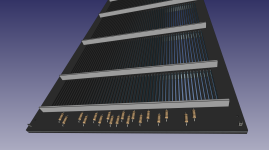
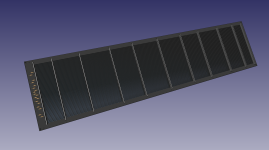
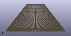
I preferred slot-style routed openings instead of holes, which would ask for horizontal stiffening means since the stiffness of the PCB needs to be taken care of.
These could be strips of PCB-material also be designed from FR4 base material, glued onto the outer side of the panel.
I could order them at the PCB-manufacturer of choice - JLCPCB seems one of the few that would accept larger than 500mm of length.
Either the inner panel side surface could be of a Masking laquer or of say a 0.5mm thick Prepreg layer to encapsulate the copper traces.
The former allows for cheap test runs using prototype manufacturing, while the latter required standard, or even special manufacturing.
Ordering 20+ pieces will probabely come even between both manufacturing processes.
Segmenting is of course very easy - it be done with resistors mounted to the PCB or on a external dedicated PCB.
Here are some pics of my designs from 2020.
What hindered me up till now to run a test were mostly time issues and the question of will the routing process of the slots maybe destroy the PCBs, because of rattle and vibration ... how would they insure that the PCB stays really fixed flat in the router?
jauu
Calvin
I also layoutet 2 different sized PCB-panels in KICAD.
I preferred slot-style routed openings instead of holes, which would ask for horizontal stiffening means since the stiffness of the PCB needs to be taken care of.
These could be strips of PCB-material also be designed from FR4 base material, glued onto the outer side of the panel.
I could order them at the PCB-manufacturer of choice - JLCPCB seems one of the few that would accept larger than 500mm of length.
Either the inner panel side surface could be of a Masking laquer or of say a 0.5mm thick Prepreg layer to encapsulate the copper traces.
The former allows for cheap test runs using prototype manufacturing, while the latter required standard, or even special manufacturing.
Ordering 20+ pieces will probabely come even between both manufacturing processes.
Segmenting is of course very easy - it be done with resistors mounted to the PCB or on a external dedicated PCB.
Here are some pics of my designs from 2020.
What hindered me up till now to run a test were mostly time issues and the question of will the routing process of the slots maybe destroy the PCBs, because of rattle and vibration ... how would they insure that the PCB stays really fixed flat in the router?
jauu
Calvin
Attachments
-
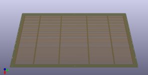
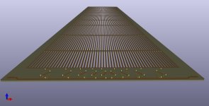 ESL-Panel - 3d 01.jpg257.4 KB · Views: 78
 -
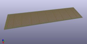 ESL-Panel - 3d 02.jpg189.2 KB · Views: 81
 -
 ESL-Panel - 3d 03.jpg180.2 KB · Views: 71
 -
 ESL-Panel - Ansicht_01.png263.5 KB · Views: 71
 -
 ESL-Panel - Ansicht_03.png226.5 KB · Views: 73
 -
 ESL-Stator - Ansicht_02.png810.5 KB · Views: 76
 -
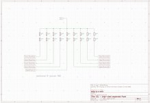 ESL-Panel - schem.JPG519.6 KB · Views: 80
 -
 ESL-MiDi-Size - 3d 01.jpg294.8 KB · Views: 74
 -
 ESL-MiDi-Size - 3d 05.jpg282.3 KB · Views: 70
 -
 ESL-midi Panel - schem.JPG524.9 KB · Views: 73
It looks like guys from HiFiMan were able to use something that looks like FR4. It's a picture of the Shangri-La Mini, which is a electrostatic headphone.
Attachments

Last edited:
i would think they use a vacuum table of some sort. i am sure pcb can work, since many already did ofcourse. so you use kicad as well. did you draw everything up in kicad or imported parts into kidac from another cad program?how would they insure that the PCB stays really fixed flat in the router?
Hey, buddy.
And what are the problems to fix a sheet of any material(?)all the central part of the glue on double-sided tape to the table, and the perimeter of the sheet to attach a special tool than you fix any other parts for processing.
As for the program for projecting, so any will do, I use Artcam.
Perforations can be made by drilling.
Here are similar works, these are parts for electrostatic headphones:
Attachments
![IMG_20241003_142526[1].jpg](/community/data/attachments/1271/1271424-4c022ae1763b432ab2853a26445b6431.jpg?hash=9zzNWLDSVa)

i made several pcb stators with my cnc (so thats not the problem), but the question i had and what the thread is about , what program one uses to in the end get a file the online PCB vendors except. i used easy eda nice for electronics not for drawing other features on a pcb. some using Kicad by the looks of it. so ill see if that can be used like a cad program, else maybe draw in my fav cad then export dxf and import in kikad, in easy eda, i can import but lining things up is terrible
so ill try some Kicad see how that works out for me 🙂
so ill try some Kicad see how that works out for me 🙂
Last edited:
Hi,
maybe they utilize some kind of vac-table maybe they don´t.
With companies like JLCPCB I assume they are rather focused on time/speed of production.
If You have delicate structures as in my design, where the slot width, resp. the ´lands´ are just a couple of mm wide but several tens of mm long,
I assume that it requires maybe a special vac-table and rather slow and soft routing.
If You have a own router at hand, then time, hence routing speed and fixing the PCb material to a base plate may not be a real issue.
then Yo may just design a PCB without routing and DIY the slots Yourself .... unfortunately I don´t .... so I have to rely on the PCB manufacturer or maybe a friendly handyman.
jauu
Calvin
KICAD is a quite mighty tool, fastly developing and growing ever more complex.
Still though the learning curve can be high and there´s a ton of third party support like vids and forums.
If You just want to do a few PCBs per Year the effort might just be a bit too much ... my colleagues learned a whole enzyclopedia of new swear words from me over the first couple of weeks 😉 ... on the other hand, its´s free of cost.
Like any other complex program it is fun when You´re using it more regularly and get familiar with all the smaller tricks.
hahaah Calvin 🙂 yeah i took a quick look Kicad might be mighty it indeed relies on knowing allot of short cuts etc. but i think its CAD capabilities are better then easyeda. yeah if you want to slot cut and the remaining material is also thin that is a problem. i dont think that would work well 🙁 only taping it down might work. i know even with vacuum the thin parts will vibrate all over the place 🙁 when you do the second slot. etc. best way would be in that case using JLC for everything, then slot cut on a home cnc. then again you could try one small panel. i mean JLC is so cheap...if you receive it all chewed up 🙂 its clear
- Home
- Loudspeakers
- Planars & Exotics
- Best software for PCB features for ESL?