As the title say, here is another one.
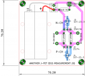
I find it convenient if battery is fixed on pcb via cable ties, no need to reverse battery polarity for N-ch and P-ch.
All other designs including a group buy pcb, needed battery polarity to be reversed.
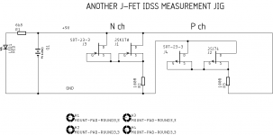
sot-23 can be DSG or SDG.
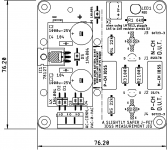
The big donuts near text N-ch idss and P-ch idss is where you connect multimeter.
regards
prasi
I find it convenient if battery is fixed on pcb via cable ties, no need to reverse battery polarity for N-ch and P-ch.
All other designs including a group buy pcb, needed battery polarity to be reversed.
sot-23 can be DSG or SDG.
The big donuts near text N-ch idss and P-ch idss is where you connect multimeter.
regards
prasi
Attachments
Last edited:
Instead of asking the user to switch the battery polarity, you ask the user to switch the multimeter connection points. A subtle difference.
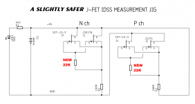
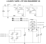
I myself have destroyed quite a few JFETs by mistakenly plugging a PJFET into the NJFET socket (or vice versa). This forward biases the gate junction, which instantly frys. Notice that your fixture can apply as much as 9V/100R = 90mA whereas the absolute max allowed gate forward current is 10mA -- see snippet from Toshiba 2SJ74 datasheet below.
My fixup for this design weakness, has been to connect a 22K resistor in series between the gate pin of the D.U.T. socket, and the rest of the circuit. This resistor has no effect when a JFET is plugged in correctly, but it prevents damage when an NJFET is erroneously plugged into the PJFET socket. And the cost is acceptably low.
_
Attachments

I saw someone's design once that soldered tightly coiled wire or springs for the transistors leads to firmly slide the transistor under test on/off the rig. It was for TO-247 and TO-03 packaging, but was a cool idea.
Instead of asking the user to switch the battery polarity, you ask the user to switch the multimeter connection points. A subtle difference.
I myself have destroyed quite a few JFETs by mistakenly plugging a PJFET into the NJFET socket (or vice versa). This forward biases the gate junction, which instantly frys. Notice that your fixture can apply as much as 9V/100R = 90mA whereas the absolute max allowed gate forward current is 10mA -- see snippet from Toshiba 2SJ74 datasheet below.
My fixup for this design weakness, has been to connect a 22K resistor in series between the gate pin of the D.U.T. socket, and the rest of the circuit. This resistor has no effect when a JFET is plugged in correctly, but it prevents damage when an NJFET is erroneously plugged into the PJFET socket. And the cost is acceptably low.
_
thanks Mark.
So a resistor between gate and source? So in case of wrongly populated N-JFET in P-ch socket, gate is more negative compared to source? and vice versa for the P-JFET
In case of corectly populated DUT, this 22k resistor effectively is a short since gate current is zero and we correctly measure I_dss.
Am I correct in my understanding?
regards
prasi
edit:
I also found a very blog by RJM that measures a few other parameters, but requires, changing of resistors depending of JFET type.
My understanding is that for all purposes (DIYA), idss measurement is more than sufficient.
Matching JFETs - diyAudio
Last edited:
This is how I connected the 22K resistors in my (somewhat different) JFET jig. In normal operation, when the FET is correctly installed, only femtoamperes flow in the 22K resistors. Thus the gate voltage is only picovolts different from the source voltage. But when the wrong polarity transistor is plugged in: the gate becomes forward biased. However the current flowing in the gate-to-source and gate-to-drain diodes, is limited to less than 0.5mA. This is well within the datasheet absolute max rating.
_
_
Attachments
Last edited:
i was trying to say same thing, but picture says thousand words. Thank you very much Mark. 
regards
prasi
regards
prasi
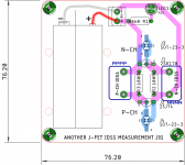
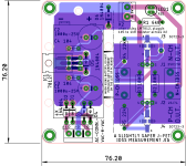
The measurement concept is marked on the PCB layout, a bit more clearly than on the schematic. View the layout in one browser window, and view the schematic in another browser window. Eureka!
I've annotated the layout with "PPPP" and "NNNN" to make this a little more clear
_
I've annotated the layout with "PPPP" and "NNNN" to make this a little more clear
_
Attachments
Nice work, Prasi. Very handy tool for the bench.
I don't know why the do-it-all transistor digital redaout testers
that are on eBay don't have the Idss feature?
Thanks,
X,
I don't know why the do-it-all transistor digital redaout testers
that are on eBay don't have the Idss feature?
Thanks,
X,
While at it, I thought why not make it somewhat more universal.
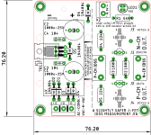
Some people may want to use a regulated supply rather than a battery for some reason. So, almost inside the battery footprint , I was able to fit-in a LM7812 regulated supply, with all variants of packages (to-220 , D-PAK and TO-92). So they can use anything thats handy.
As per Mark's annotation, I have renamed the jig as "A slightly safer JFET I_dss measurement jig". 🙂. Also used his " round box ", of actual measurement location. Looks nice!🙂
regards
prasi
Attachments

To provide sockets / footprints / test sites for several different pinouts and packages. Only a single JFET is installed at any one time, in the most convenient position. All other positions are left empty.
- Home
- Amplifiers
- Solid State
- Another Idss measurement jig