Any suggestion. I can’t adjust the offset setting in the left channel of the rec. differential amplifier. In SM should be up to `+/-10mV, but in fact the voltage in TP1 fluctuates after fine tuning in a couple of minutes from 5mV to 60mV? Was checked transistors TR,25,26 replaced TR24 and electrolytes C6,7.
Attachments
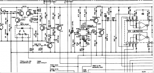

All voltages in both channels are the same as the in diagram. Defect start after several minutes after power on.
Sorry I'm not understood. Can you tell me more about DC return? The thermal derivative in the other channel is normal , off-set is stable. Will replace potentiometer.
Can you suggest possible reasonsPerhaps there is a conductive path from TP1 and right JFET's gate. (Say, a resistance or a coil not shown in the piece of schematic above depicted).
R89 91 is okCheck R89. As its high valued, it may be deffective.
BINGO !!! C9 defective ! Capacitance decrease !TR 27 & 28? Seems they are using them as switches. D8 is a varicap an is DC isolated from TP1 node.
Many thanks for the help !!!Is it leacky? A decreasd cap value can't modify any DC value...
Yes the drift disappeared , now all voltages in both channels are stable.Does the drift dissapear?
- Home
- Source & Line
- Analogue Source
- AKAI GX-F91 REC DIFFERENTIAL AMPLIFIER OFF-SET