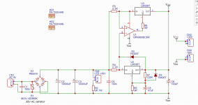
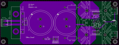
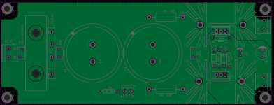
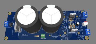
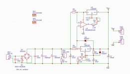
Attached is the schematics and gerber files for anyone who wants to build this.
Rectifier bridge heatsink - HSS08-B18-CP
Heat sink clip for H SS08-B18-CP - HSC-06
Heatsinks for LM338 - FA-T220-64E
Any suggestions on layout improvements or schematics are welcome and appreciated!
Rectifier bridge heatsink - HSS08-B18-CP
Heat sink clip for H SS08-B18-CP - HSC-06
Heatsinks for LM338 - FA-T220-64E
Any suggestions on layout improvements or schematics are welcome and appreciated!
Attachments
A clever way to share the current load! You could extend the idea to multiply the current, and use a power transtor(s) instead of a second LM338. Maybe I will throw up a simulation to illustrate. Later. Only suggestion is that U1 could be powered from ahead of the 0.1 Ohm resistors.
Linear power supplies are not rocket science, and I would just use a power transistor and a few other parts. Foldback and/or shut-down make it bulletproof if you intend it use it as a bench supply.
Linear power supplies are not rocket science, and I would just use a power transistor and a few other parts. Foldback and/or shut-down make it bulletproof if you intend it use it as a bench supply.
And while OPA990 is good for an exceptional 40V, you could use lower voltage op-amps if you drop the negative supply to the op-amp. It has to be about 3V below the output. Designs that use exotic parts are a future PITA. For a modest application, I would stick to common parts.
A clever way to share the current load!
Thank you! I took the idea from the datasheet 🙂 (I am not smart like that in electronics yet)
That can be done, I suppose...Only suggestion is that U1 could be powered from ahead of the 0.1 Ohm resistors.
I am not sure what "Foldback and/or shut-down" means 🤔Foldback and/or shut-down make it bulletproof if you intend it use it as a bench supply.
I googled replacement for LM107 and found this: "This circuit can use any high-voltage opamp whose input common-mode range includes the positive rail. This is not true for the LM741, but the OPA990 will work."And while OPA990 is good for an exceptional 40V, you could use lower voltage op-amps if you drop the negative supply to the op-amp. It has to be about 3V below the output. Designs that use exotic parts are a future PITA. For a modest application, I would stick to common parts.
I don't understand what "input common-mode range includes the positive rail" means, so I went with the suggested OPA990. If you can suggest any other common OPAMP I would rather go for that.
Will something like IRFB3607PBF work? Any suggestions on a transistor?Linear power supplies are not rocket science, and I would just use a power transistor and a few other parts.
I googled little more and it seems like good option will be to use NMOS type of transistors for linear voltage regulation.
Few transistors available on Mouser:
FDP86363-F085 - 80V / 110A - $3.64
FCH104N60F-F085 - 600V / 37A - $6.57
IRFB3607PBF - 75V / 80A - $1.42
And for voltage regulators:
LM338T - 32V /5A - $2.45
Few transistors available on Mouser:
FDP86363-F085 - 80V / 110A - $3.64
FCH104N60F-F085 - 600V / 37A - $6.57
IRFB3607PBF - 75V / 80A - $1.42
And for voltage regulators:
LM338T - 32V /5A - $2.45
Last edited:
Attached is another revision with voltage adjustment trim pots. I included pads to probe ADJ pins for LM338 regulators.
I wonder if there is a way to independently adjust voltage output for each regulator?
I wonder if there is a way to independently adjust voltage output for each regulator?
Attachments

R9 won't 'adjust the voltage' of U3 - it's output voltage is defined by the output of U2, whilst the active feedback due to U1 ensures equal current sharing between the two regulators. Varying R9 will merely vary the voltage between U3 adjust and U1 output.
Last edited:
Does this mean I can get rid of R9?R9 won't 'adjust the voltage' of U3 - it's output voltage is defined by the output of U2, whilst the active feedback due to U1 ensures equal current sharing between the two regulators. Varying R9 will merely vary the voltage between U3 adjust and U1 output.
And set the R7 to 2.9k or so - close to get output voltage of 32V?
I am not trying to build adjustable voltage regulator. Just wanted to trim output voltage +-1V or so.
If you put the power on LED to the output you'll have your minimum load and a proof the PSU is working. The loss to useless heat will be considerable, one would think LDO regulators like LT1084 to be a better choice.
If you can get these parts, then go with the reference design. The FET you mentioned could make a pass transistor, but the gate voltage would have to be about 6 Volts higher than the LM338 ADJ pin, which could be problem if the raw voltage was not high enough. I shouldn't suggest you attempt something more complicated. The 2nd LM338 is acting as a depletion mode FET pass transistor, ie the input voltage is below the output/source voltage.
Common mode range is the voltage range where the inputs operate properly, which is not typically beyond nor near the supply voltage. In this circuit, the input pins 1,3 sit at a voltage at or above the power supply pin5. That is why I suggested connecting 5 ahead of the 0.1 Ohm resistors.
As others have pointed out, the 2nd LM338 mirrors the current in the first regardless of the output voltage and the first LM338 sets the voltage.

Thanks for the explanation! It truly helped to understand these more.Common mode range is the voltage range where the inputs operate properly, which is not typically beyond nor near the supply voltage. In this circuit, the input pins 1,3 sit at a voltage at or above the power supply pin5. That is why I suggested connecting 5 ahead of the 0.1 Ohm resistors.
As others have pointed out, the 2nd LM338 mirrors the current in the first regardless of the output voltage and the first LM338 sets the voltage.
I made some changes based on those two points. Did I get it right?
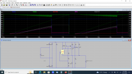
Yes, but I also see a 25VAC input, which is not enough for a clean 30VDC out at more than about an amp. I probably shouldn't complicate your life, but here is a similar circuit I threw up in SPICE. Spice tells you all kinds of great information, like the need for a substantial raw supply, stability issues, etc. If you don't already, you should spend some time using SPICE. LTC Spice is free and many people at DIYA use it.
Note:
1. a 30VAC (42VP) input is just enough with 20,000uF bulk caps for 30VDC out at 10A.
2. Q3 is "VI" protection for the pass transistors and leaves the LT1117 (~LM317) to its own current limit at about 12 Amps total output (see traces).
3. R7, and the lack of any caps (like your C6) on the ADJ pin are important for stability.
4. Most of these 3 terminal regulators are limited to about 30V, which could be a problem if they were shorted so that more than 30V was across in and out.
5. If you use a high current chip like LM338, then you don't need Q4.
6. The VI protection resistor(s) R8 (and R9) blead current and can cause the output to raise above 30V if the supply is unloaded, but if you make them too high value to reduce that current, then the VI protection suffers. The best thing about using LM338s is that they have their own protection built in.
Attachments
Ideally I want to have two different options for voltage out: 28V at 7A and 36V at 9A with the ability to trim +-2V
I assume discrete design should allow for more flexibility to achieve that.
Regarding two LM338 board:
I think that I need 28V AC from 400VA transformer to be able to get 32V out.
Or 24V AC from 300VA transformer to get 28V.
I have LTSpice installed - I will try playing with the design but will take me some time to understand how it works.
- Home
- Amplifiers
- Power Supplies
- 10A linear power supply rectifier board with 2xLM338 regulators