Hi,
Could someone, please, explain to me why can be seen on some design, fast op amp loaded to ground with a resistor and // capacitor before the RCA output after a serie Rsio of an opamp that already isolate it from the "true" load of the next stage ? Is it for even more stability and capacitive load ?
It's about a transimpedance circuit of a source, towards a preamp. On the preamp side it is terminated with 220R serie rigth at the input with 47K shunt and a couple of hundred pF cap to Ref as well. transmission line is a typical said 50 ohms RCA cable !
Thanks
It has nothing to do with transmission line effects. Audio frequency signals aren't fast enough. Think about it: the speed of light is 3E8 meters/second. In free space a 20KHz (2E4 Hz) signal has a wavelength of 1.5E4 meters. 15 kilometers! OK, the propagation of a signal down a cable is slower: but not enough so to make a substantial difference in this regard. Considering a 2 meter cable, back reflections due to impedance mismatch will look pretty much the same as the incident wave -- they haven't changed to any measurable amount, so they will have no impact on the signal.
It is all about keeping RF out of the active circuitry. Stuff like the local radio station, your wireless router, cell phone transmissions etc. There has been a lot of discussion on various threads regarding this issue. Consensus is that stray RF is everywhere so it's got to be dealt with in order to avoid problems.
It is all about keeping RF out of the active circuitry. Stuff like the local radio station, your wireless router, cell phone transmissions etc. There has been a lot of discussion on various threads regarding this issue. Consensus is that stray RF is everywhere so it's got to be dealt with in order to avoid problems.

Actually some audio circuits can oscillate at tens of megahertz and when they do, it seriously affects their audio performance. The RC network at the preamplifier input may help to keep it stable despite transmission line resonances.
That said, I agree with Mark that the main purpose is probably to improve immunity to RF signals.
That said, I agree with Mark that the main purpose is probably to improve immunity to RF signals.
Do we talk about the input of the pre of my illustration or about the output load before the Rca of the source device before ?
In my example, it is about a dac output current and a transimpedance op amp. So the Rfb//CfB gives a 6 dB filter that is too weak so the tens of Mghz and their peaks still matter. The serie Rsout at the output (10R ro 50R often) isolate partially from the load.
SO what exactly do the 47K // 100 pF shunted to ground and just before the RCA plug, so on the same pcb of the dac & op amp ?
Is it to shunt to ground the nasty RF ? 47k // 100 pF gives the corner frequency of the RF attenuation or the 47K is just there for impedance and the cap for RF only .... then again same on the pre input (but 220 R serie input with re 47K to Ref for the load impedance and 220 pF for the RF to ground ?
Last edited:
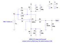
this is the shematic I try to understand more . Initialy I thougth the 47K//100 pF to Ref was for the sim only and simed the next stage input (preamp). But it seems to be on the dac pcb, hence my questions.
The AD811 has high bandwith as a video CFB amp, up to 100 Mhz and a high slew rate of 2500V/s , don't remember of Aol...
Should I consider RF from the beginning with any op amp cause the nasty RF of dac chip current outputs ? And anyway load at op amps output near its output pin layout wise? (My understanding is I need at least 20V/S slew rate for 16 bits and preferabily 50 M hz for correct dac chip I to V conversion)
Attachments
Last edited:
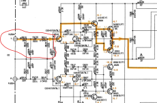
and here is the input pre stage I have. so 100K R//100K R gives the 50K load I assume.
Attachments
Last edited:
Do we talk about the input of the pre of my illustration or about the output load before the Rca of the source device before ?
In my example, it is about a dac output current and a transimpedance op amp. So the Rfb//CfB gives a 6 dB filter that is too weak so the tens of Mghz and their peaks still matter. The serie Rsout at the output (10R ro 50R often) isolate partially from the load.
SO what exactly do the 47K // 100 pF shunted to ground and just before the RCA plug, so on the same pcb of the dac & op amp ?
Is it to shunt to ground the nasty RF ? 47k // 100 pF gives the corner frequency of the RF attenuation or the 47K is just there for impedance and the cap for RF only .... then again same on the pre input (but 220 R serie input with re 47K to Ref for the load impedance and 220 pF for the RF to ground ?
The 47 kohm or 49.9 kohm does essentially nothing when the circuit is on. Maybe it's there to keep the output at ground level when the circuit is off, or during turn-on or turn-off? I don't know.
Whether the 10 ohm-100 pF is there to filter the output signal (keep high frequencies from going out of the box) or for RF immunity (keep high frequencies from entering the box) or both, I also don't know. It will act as a filter in both directions: from voltage from the op-amp to voltage across the connector and from current through the connector to current through the op-amp output.
and here is the input pre stage I have. so 100K R//100K R gives the 50K load I assume.
This helps to keep Q516 and Q518 from unintendedly demodulating RF signals, if there are any at the input connector. It may also help to prevent instability when there is a cable connected to the input that is shorted or open at the other side. My guess would be that it's mostly there for RF immunity.
Many thanks Marcel. I hope @grunf will enligth us about why he putted that 100 pF and mainly this 49.5K to ground from hid point of view.
I thougth it was for the sim and was copping to the datasheet AD811 inputs, but if the 100 pF is there physically near the AD811 output on the pcb for the RF in the direction you and @Mark'51 input, it is surely mandatory. the Vout is after on the shematic of the datasheet and >i didn't understand if it was only supposed to be the capacitance of the pcb layout to ground.
Btw, the input stage of the CX-2 Yamaha pre you see is the the one of the CD input and the pre after is fulll discrete till the output.
Here the datasheet that speaks about the 10 R and the 100 pF load on the AD811 : (the datasheet shows voltage gain but the feedback loop is the same (inverting input) with the transimpedance virtual ground instead with at least same Rfb value but more Cfb value story I assume to have a larger flat impedance in the I/V node and at the same time to lowish the corner frequency output roll off very early because we use NOS and no reconstruction filter... and having also less ripple at output in the audio bandwith as per datasheet explanation. At least it is my basic understanding. Thanks again for that RF tip learning. 🙂, it was not clear to me if the datasheet assumed the 100 pF was an average load of the next stage in a video transmission line for illustration or not.
Last edited:
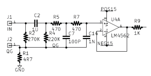
Here's the input of the "Super Gain Clone" designed by Bob Cordell and presented in his book Designing Audio Power Amplifiers. The Table Of Contents contains an entry named The Super Gain Clone, appropriately enough, in both paper editions and in all Kindle Reader editions. That'll tell you the page number in your copy, if you wish to read everything Bob has to say about the design.
_
Bob Cordell said:The amplifier begins with the usual 4.7 ohm resistor that isolates analog ground from circuit ground so as to prevent ground loops. A passive LowPasssFilter input network provides two poles of roll-off and minimizes RFI ingress. U4a is a conventional noninverting unity gain buffer employing half of a dual op-amp.
_
Attachments
- Home
- Source & Line
- Analog Line Level
- About loading a fast opamp at its output before the transmission line, help needed