Hi everyone,
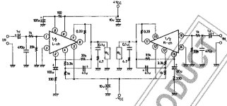
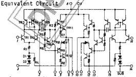
I'm trying to build this amplifier based on the Sanyo STK465 amplifying module (I attached the originals down below).
And this is my version:

I simulated this circuit using LTspice and everything works as I expected. I attached the simulation down below.
The problem is that when I build it in real life the DC bias point of the output stage is not going to 0V DC. It sits close to the positive rail and I can't figure out the reason. I can't proceed further until I get the DC bias point right, so I'm stuck here.
I'm currently using a 10K resistor as the load so i don't fry the output transistors, but the problem persists even with a 10 ohm load. R6 and R7 are there to protect the output transistors as well.
What I tried:
I'm at a loss. Why doesn't the VAS stage bias the Sziklai pairs in the output stage correctly? Do you have any suggestions? Thank you very much for your time and for your help.
I'm trying to build this amplifier based on the Sanyo STK465 amplifying module (I attached the originals down below).
And this is my version:
I simulated this circuit using LTspice and everything works as I expected. I attached the simulation down below.
The problem is that when I build it in real life the DC bias point of the output stage is not going to 0V DC. It sits close to the positive rail and I can't figure out the reason. I can't proceed further until I get the DC bias point right, so I'm stuck here.
I'm currently using a 10K resistor as the load so i don't fry the output transistors, but the problem persists even with a 10 ohm load. R6 and R7 are there to protect the output transistors as well.
What I tried:
- I checked the supply rails and they are fine. They come from a dual power supply I built which uses L7812CV and L7912CV linear regulator.
- I checked the connections a thousand times.
- Tried to remove all capacitors (excluding the decoupling ones and the compensation capacitor C4) in order to focus on the DC response only.
- The circuit was originally built on a breadboard. I've now soldered the amplifier on a perf board, while the rest of the circuit (the input section, the output filter, the feedback) is still on the breadboard.
- I put a 10K potentiometer on the emitter of Q5 and tried to trim it (therefore decreasing the gain of the VAS stage) until I got 0V DC at the output. I couldn't get it to work: as I got closer and closer to zero, the output flipped to the negative rail; I then trimmed the pot on the opposite direction, and the output flipped back to the positive rail. I think this happens because Q5 gets shut completely off, causing the output to swing to the negative rail.
I'm at a loss. Why doesn't the VAS stage bias the Sziklai pairs in the output stage correctly? Do you have any suggestions? Thank you very much for your time and for your help.
Attachments
Last edited:
I had a similar problem with a similar topology. After hours of cursing, it turned out I have swapped a PNP and an NPN. Did it work on breadboard?
I just checked and the transistors are in their place. No, it didn't work on breadboard either. I actually built it twice, one time in the university lab and then again at home. Still didn't work.
D1 is a zener to generate a fixed reference voltage (I chose -5.6V) to bias the differential pair in the input stage. It's oriented in the same way as in the original schematic, and it's actually working as expected. It measured the expected -5.6V on the real circuit without problems.
D1 is a zener to generate a fixed reference voltage (I chose -5.6V) to bias the differential pair in the input stage. It's oriented in the same way as in the original schematic, and it's actually working as expected. It measured the expected -5.6V on the real circuit without problems.
Last edited:
To be fair, I don't know exactly. I focused on the DC feedback only. Still, if I remove C1 the DC point of the circuit doesn't work anyways, I already tried.
In order to try to answer your question I tried to simulate the AC response with and without C1, here they are.
With C1:

Without C1:

C1 seems to lower the gain a bit with no significant action on the phase and that's it.
In order to try to answer your question I tried to simulate the AC response with and without C1, here they are.
With C1:
Without C1:
C1 seems to lower the gain a bit with no significant action on the phase and that's it.
I tried with an oscilloscope and it's not oscillating, it's nailed to the positive rail with a pure DC voltage.
Furthermore, yesterday out of desperation I also tried the following:
I know it wasn't logical, but it had already tried everything. I also know the original schematic by Sanyo is correct, as variations of this topology are widely used.
Furthermore, yesterday out of desperation I also tried the following:
- I removed C1, R8 and C5, leaving only R4 in the feedback network
- I swapped the inputs of the differential couple (input signal to the inverting input, feedback to the noninverting input) thinking that maybe the original schematic was wrong
- I trimmed the emitter potentiometer of Q5 mentioned above in order to have 0V DC at the output (and this time, to my surprise, it was stable!)
- I put a sine wave in the input (now at the inverting input of the diffential couple), scoped the load resistor and saw the same sine wave (obviously it wasn't 40dB bigger wrt the input, as I had disconnected C5 and R8; only R4 was present in the feedback network)
- I then reconnected C1 and R8. The output sine wave disappeared, and the output at the load became completely unstable
I know it wasn't logical, but it had already tried everything. I also know the original schematic by Sanyo is correct, as variations of this topology are widely used.
Are you sure your output devices are still healthy? If you don't have everything, including the bias diodes, mounted on a heatsink, your design is very susceptible to thermal runaway. 90mA is quite a lot of bias current and you'll quickly get into a thermal runaway condition that will destroy one or both of your output transistors.
i also wonder about the output devices - no emitter resistors (or collector resistors in this CFP configuration) - yikes! This is all discretes now (instead of a module that provides nice temp tracking of semiconductors) - you need to account for that ....
maybe 1st, make sure the diff and VAS are OK by dropping the output stage and closing the feedback loop with R4 at junction of D2 and D3....
maybe 1st, make sure the diff and VAS are OK by dropping the output stage and closing the feedback loop with R4 at junction of D2 and D3....
I would address the potential thermal runaway by replacing the diodes with a VBE multiplier. You should mount that BD139 on the same heatsink at the outputs. This also makes it easy to adjust the bias by replacing R12 with a potentiometer and a series resistor. Something like this:

Thank you very much for your suggestions, they are much appreciated.
Actually in an earlier stage of the project I didn't include the BD140 and BD139 and kept the load to an high impedance (10k-100k ohms) to test if the circuit was working at all without worrying too much about thermal runaway. I also kept R6-R7 to 10k for the same reason. Still, as before, it worked in simulation but not in reality. To be honest, yesterday I got fed up (and senseless), put my caution aside and pushed ahead by including the output Sziklai pairs and going full power.
I'll check if the transistors are okay as soon as I can, hopefully tonight. I'll to drop the output stage and close the loop between D2 and D3 to check the VAS.
Finally, I actually dropped the VBE multiplier on purpose to simplify the design in order to debug it. I'll reinstall it with the potentiometer and try again.
Thanks again to both.
This is really strange. The design is very straightforward. I'll build it up on breadboard myself tonight if I get time.Still, as before, it worked in simulation but not in reality.
It must be oscillating. The Vbe of Q6 is about 20mv while the Vbe of Q7 is about 1.2v and those are not correct values for a linear biased transistor. The Q6 and Q9 configuration is prone to oscillation because there is significant phase shift between Q9's collector and base voltage since PNPs are at least 3 times slower than NPNs.
That's not the normal CFP topology - the power devices should have ~100 ohm resistors between base and emitter, and probably a few ohms of stopper-resistance on the base.
You will probably need the equivalent of emitter resistors between output devices and output for thermal stability of bias point.
You will probably need the equivalent of emitter resistors between output devices and output for thermal stability of bias point.
- Home
- Amplifiers
- Solid State
- Completely wrong DC bias on output stage