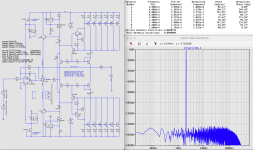
This split-Mirror Diamond (sMD) amplifier is a bipolar multi-nested feedback amplifier designed using LTSpice. It is intended as a redesign and reconstruction on a Nakamichi PA-5 chassis that can support the numbers of output devices indicated with its +/- 60 Volt supplies. The amplifier uses two operational amplifiers, an LTC6090-5 high voltage input amplifier to provide voltage gain of ~14dB and an LT1022 amplifier with output tracking supplies that controls the diamond. The power output network uses multi-paralleled bipolar devices. These interact with 4 high current BIPOLAR devices Q1/Q2 as inputs and Q3/Q4 connected as diodes.
The input devices Q1/Q2 are fed from constant current sources by two power MOSFET’s M5 and M6 feeding about 90mA to the input side of the diamond. This current is mirrored in the output Q3/Q4 devices, being thermally connected to the input Q1/Q2 devices to support thermal tracking of the set point quiescent current. The dissipation is about 25 Watts idling/channel, hence not a low quiescent amplifier. Also included is a current limiting protection network that supports a 200W/4 Ohm load.
As a caveat it should be noted that many operational amplifiers are not modeled for distortion and that the total harmonic distortions numbers indicated are not trustworthy. Notwithstanding the realities the harmonic distortion spectral components simulated are all of amplitude beneath the noise floor for all power levels to 200W/4R at a more difficult frequency of 2kHz. In the screenshots the 0dB value represents 28.4 V RMS that supports 200W/4R or 100W/8R.
Again, I would like to thank Hans Polak for his help in using LTSpice and for his examination and input on the network design.
Attachments

To add. Below shows the power supply sources to the LT1022 in relation to the potential difference across the split Mirror Diamond (sMD at full power 1kHz - 200W/4R. Note that the input/output across the sMD is nearly overlapping in the center, also with the LT1022 output operating nicely near mid-supply within the voltage tracking boundaries.

Below is the voltage out across the load in relation to the current out of the LT1022 while voltage tracking the sinusoid under circumstances as per the above. The peaking of the current is the result of loop feedback correction in response to nearing the current limiters at full power 200W/4 Ohm. The current limiters being set to about 12.5 Amps with full power peak current being 10 Amps at 200W/4 Ohm. As observed on the right these currents effectively disappear when current limiting resistors R9/R10 are reduced by an order of magnitude as would then require 125 Amps to limit.


Operational amplifier U1 is the global feedback device operating as integrator with a 68pf feedback capacitor, effectively appearing across the 10k Ohm feedback resistor that sets the bandwidth. The current output of U1 is shown in relation to the output voltage of the amplifie, as observable at a 90 degree phase shift, hence purely capacitively loaded. Of note is that at 1k Hz the output current of U1 is in the order of +/-20uA, meaning U1 is operating largely unloaded, a condition supporting low distortion in itself, and that in conjunction with high voltage supplies keeps the dissipation to a bare minimum. Observable in the network is that the output is directly connected to the inverting terminal of the LT1022, hence in configuration a unity gain loop feedback connection that in the absence of a need for integration for stability operates in a high speed time alignment way, this as observable by current drive correction above. This is while the positive input terminal of the LT1022 is changing more slowly, being driven of overall loop integration correction by U1. This combination of dual loop feedback correction as feedback nesting, in conjunction with added benefits that the sMD with further feedback nesting is largely responsible for ultra-low distortion results.

Below is the voltage out across the load in relation to the current out of the LT1022 while voltage tracking the sinusoid under circumstances as per the above. The peaking of the current is the result of loop feedback correction in response to nearing the current limiters at full power 200W/4 Ohm. The current limiters being set to about 12.5 Amps with full power peak current being 10 Amps at 200W/4 Ohm. As observed on the right these currents effectively disappear when current limiting resistors R9/R10 are reduced by an order of magnitude as would then require 125 Amps to limit.
Operational amplifier U1 is the global feedback device operating as integrator with a 68pf feedback capacitor, effectively appearing across the 10k Ohm feedback resistor that sets the bandwidth. The current output of U1 is shown in relation to the output voltage of the amplifie, as observable at a 90 degree phase shift, hence purely capacitively loaded. Of note is that at 1k Hz the output current of U1 is in the order of +/-20uA, meaning U1 is operating largely unloaded, a condition supporting low distortion in itself, and that in conjunction with high voltage supplies keeps the dissipation to a bare minimum. Observable in the network is that the output is directly connected to the inverting terminal of the LT1022, hence in configuration a unity gain loop feedback connection that in the absence of a need for integration for stability operates in a high speed time alignment way, this as observable by current drive correction above. This is while the positive input terminal of the LT1022 is changing more slowly, being driven of overall loop integration correction by U1. This combination of dual loop feedback correction as feedback nesting, in conjunction with added benefits that the sMD with further feedback nesting is largely responsible for ultra-low distortion results.
Interesting, but the LTC6090 have a quite tricky capsule with a soldering pad for heat spreading.
Have you checked if the dissipation is so large that it is needed?
Have you checked if the dissipation is so large that it is needed?
I have these devices already and know about the soldering pad on the bottom. I don't plan on doing anything with the heat spreading pad as yet, mainly because I don't think it necessary given what can be considered the complete unloading of its output. The option is just to glue a little heatsink to the lid on top as suspected will be more than enough under the circumstances. The plan is to solder this device to a soic to dip converter as I have other high voltage op-amp devices as well in dip's that I want to experiment with.
Just checked. It's about 3mA supply at what will be about 100 Volt total supply, hence about 300mW no load. So should be fine.
Just checked. It's about 3mA supply at what will be about 100 Volt total supply, hence about 300mW no load. So should be fine.
Last edited:
Ok, I didnt study the schematic in full, neither the datasheet so I dont have a grasp of the quiscent power loss or as you say load-related power loss. But if you considered it that is fine. Interensting setup anyhow.
Heatsink om top helps but not so much due to Junction to case resistance.
Soldering pads can also spread heat.
Heatsink om top helps but not so much due to Junction to case resistance.
Soldering pads can also spread heat.
Thx Jan,
To divert for a bit the most interesting and time consuming was the design and construction of an autonomous micro-mouse robot shown below, taking 800 + hours to bulid split between hardware and software. This was in the late 90's for a micro-mouse competition held at the American Power Electronics Convention in Dallas Texas. I was sponsored by David Otten the organizer from MIT whose own robots are pictured in the upper left and right. His robot in the upper right beat mine by one spot, he came in fourth in an international field. Mine was by far the smallest, lightest and lowest SG of all the competitors. It fit into my shirt pocket.

It operated on dual HC12 Motorola microcontrollers, communicating between each other on the upper and lower boards. The upper board performed high speed A/D conversions of IR sensors synchronized to high current ~1A strobed IR emitters. A day before the event the laptop diagnostic interface created for it showed my front IR LED was blown for some reason, as fortunate to have a spare and replace. The upper controller also contains a maze solving flooding algorithm that was written by a brilliant 4th year student, someone who was taking a concurrent degree in Electrical Engineering and Computer Science. This controller also gathered from the bottom controller and sent data via the removable RF transmitter on the top to the diagnostic device.
The lower board HC12 microcontroller performed the motor control functions for the wheel-chair style drive. Each motor with high speed quadrature encoders for distance motion and the input for a cross-linked speed/steering feedback control system. It also contained the numerous arcing routines with speed/acceleration profiling for variant runs in attempting to go faster. All of routines where in a binder full of VISIO flowcharts to organize.
Hopefully this diversion wasn't too boring...
To divert for a bit the most interesting and time consuming was the design and construction of an autonomous micro-mouse robot shown below, taking 800 + hours to bulid split between hardware and software. This was in the late 90's for a micro-mouse competition held at the American Power Electronics Convention in Dallas Texas. I was sponsored by David Otten the organizer from MIT whose own robots are pictured in the upper left and right. His robot in the upper right beat mine by one spot, he came in fourth in an international field. Mine was by far the smallest, lightest and lowest SG of all the competitors. It fit into my shirt pocket.
It operated on dual HC12 Motorola microcontrollers, communicating between each other on the upper and lower boards. The upper board performed high speed A/D conversions of IR sensors synchronized to high current ~1A strobed IR emitters. A day before the event the laptop diagnostic interface created for it showed my front IR LED was blown for some reason, as fortunate to have a spare and replace. The upper controller also contains a maze solving flooding algorithm that was written by a brilliant 4th year student, someone who was taking a concurrent degree in Electrical Engineering and Computer Science. This controller also gathered from the bottom controller and sent data via the removable RF transmitter on the top to the diagnostic device.
The lower board HC12 microcontroller performed the motor control functions for the wheel-chair style drive. Each motor with high speed quadrature encoders for distance motion and the input for a cross-linked speed/steering feedback control system. It also contained the numerous arcing routines with speed/acceleration profiling for variant runs in attempting to go faster. All of routines where in a binder full of VISIO flowcharts to organize.
Hopefully this diversion wasn't too boring...
Last edited:
A bit more diversion before getting back. I found a couple Youtube videos on the micro-mouse Jan.
David Otten is now up to MITEE 13 in the first video, up from MITEE 3 above. Looks he's been busy (he's the bald one... but extremely nice for being so bald). The video below it is a general history that shows a flooding algorithm at about time 8:46. Interesting stuff what they are up to 20 years later.
Gerrit
Last edited:
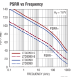
An aspect of power amplifier design considered more critical than perhaps realized is the PSRR, particularly under circumstances whereupon distortion that is particularly low can be influenced more by the power supply. As a result, particular attention was also focused on measures to mitigate the risk of sonic consequences as related to PSRR. This is not to suggest that the extent of PSRR realized is either necessary or sufficient.
Simulations revealed that supply regulation of the LTC6090 input op-amp is particularly critical. This was determined by a number of simulations applying a 1 Volt test signal inserted in series with the positive power supply rail. In the first simulation below left is with the input LTC6090 removed, with the positive input to the LT1022 grounded, thus testing only the PSRR of the output amplifier in a unity gain buffer mode, and with the LT1022 still in the loop to control the sMD. The PSRR results appear reasonably impressive. The reason for this performance is that the tracking supplies also provide pre-regulation to the LT1022, forming an isolation layer from the raw supplies, being further reduced by the PSRR of the LT1022 itself, and thot for reasons operating in a broadband unity gain feedback loop way pushes the PSRR frequency extension. The simulation to the right once again includes the LTC6090. Observable is that the PSRR is worse, as counter to what can be expected.


The reason for this is that the input regulation to the LTC6090 is inadequate, that in being so becomes dominant of the overall PSRR. Ultimately failing by the use of the JFET's in the supplies. In the notes on the schematic (this near these JFETs) indicates replacement by NSIC2020's. These are 120 volt rated LED drivers as constant current sources fixed at 20mA. These appear ideally suited for this application. Given the voltage range of NSIC's the current regulation can be expected exceptional, even though untested. In the simulation below left, the NSIC's are simulated by ideal current sources, improving PSRR broadband by a minimum of 20dB at 20kHz. This can now be compared to an input LTC6090, operating with an unregulated supply to the right.


What is evident is the serious degradation in the PSRR to exclude regulation, being not worthy of the risk to sonics to exclude
Gerrit
Simulations revealed that supply regulation of the LTC6090 input op-amp is particularly critical. This was determined by a number of simulations applying a 1 Volt test signal inserted in series with the positive power supply rail. In the first simulation below left is with the input LTC6090 removed, with the positive input to the LT1022 grounded, thus testing only the PSRR of the output amplifier in a unity gain buffer mode, and with the LT1022 still in the loop to control the sMD. The PSRR results appear reasonably impressive. The reason for this performance is that the tracking supplies also provide pre-regulation to the LT1022, forming an isolation layer from the raw supplies, being further reduced by the PSRR of the LT1022 itself, and thot for reasons operating in a broadband unity gain feedback loop way pushes the PSRR frequency extension. The simulation to the right once again includes the LTC6090. Observable is that the PSRR is worse, as counter to what can be expected.
The reason for this is that the input regulation to the LTC6090 is inadequate, that in being so becomes dominant of the overall PSRR. Ultimately failing by the use of the JFET's in the supplies. In the notes on the schematic (this near these JFETs) indicates replacement by NSIC2020's. These are 120 volt rated LED drivers as constant current sources fixed at 20mA. These appear ideally suited for this application. Given the voltage range of NSIC's the current regulation can be expected exceptional, even though untested. In the simulation below left, the NSIC's are simulated by ideal current sources, improving PSRR broadband by a minimum of 20dB at 20kHz. This can now be compared to an input LTC6090, operating with an unregulated supply to the right.
What is evident is the serious degradation in the PSRR to exclude regulation, being not worthy of the risk to sonics to exclude
Gerrit
Last edited:
This is an unexpected result, as you ,emtioned, and thus should be scrutinized. PSRR for almost any opamp, including this one, is huge.
I wonder to what extend the LTspice model does accurately follow the real thing. Not sure the PSRR is even included in the model.
Jan
I wonder to what extend the LTspice model does accurately follow the real thing. Not sure the PSRR is even included in the model.
Jan
Attachments

Jan,I wonder to what extend the LTspice model does accurately follow the real thing. Not sure the PSRR is even included in the model.
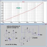
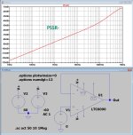
Here are the simmed PSSR+ and PSSR- with Av=1V/V
Both are identical in the sim.
The PSSR- is relatively accurate, but the PSSR+ is 40dB too pessimistic in the sim.
Hans
Attachments
It should be noted that the sMD or "split mirror diamond" is also a feedback network, though discreet, this with its own PSRR. This is shown below left with its input grounded through R14 on its input. This then being nested inside the loop of the LT1022 that reduces the overall PSRR as again below middle, and then both nested again by the input integrator on the right, hence the form of the multi-nested feedback indicated in the initial post.


Gerrit
Gerrit
Last edited:
So it looks like they just plugged the same number for +psrr and -psrr in the model.The PSSR- is relatively accurate, but the PSSR+ is 40dB too pessimistic in the sim.
Normally +psrr is (much) better than the -psrr as you discovered.
Jan
I'm hoping the added regulation will be sufficient in conjunction with whatever PSRR's of the LTC6090's happen to be as good enough Jan.
To continue some, as an overview of the whole of the amp, their was an intention to support the possibility of bridging in creating a mono-block, whereupon the numbers of output devices are viewed possibly adequate to support this.
In a bridged mode with a 4 Ohm load the impedance seen by each half (as left/right channels) reduces to 2 Ohm's. This can be imagined that the midpoint of a 4 Ohm load swinging differentially on either side is pivoting at its center about a virtual ground as thereupon appearing 2 Ohms. In testing at 28.4V RMS with a more difficult 2 Ohm load, the power increases to about 400Watts/2R per half, or then 800W/4R total in balanced The distortion levels tested on one side at 2 Ohms seems likely of little difference in the bridging as 4R across the bridge.

For interest (as also for the amusement) this amplifier was also simulated for a lower 2 Ohm load, as then only 1 Ohm to ground per side, that for a 28.4V RMS signal across the 1 Ohm, represents 28.4A RMS or ultimately 1600W/2R. The distortion levels appears with all spectral distortion components still below -140dB. Bear in mind that this is unrealistic to consider can be achieved to this extent in any reality, as seems the potential for blowing smoke.

Gerrit
To continue some, as an overview of the whole of the amp, their was an intention to support the possibility of bridging in creating a mono-block, whereupon the numbers of output devices are viewed possibly adequate to support this.
In a bridged mode with a 4 Ohm load the impedance seen by each half (as left/right channels) reduces to 2 Ohm's. This can be imagined that the midpoint of a 4 Ohm load swinging differentially on either side is pivoting at its center about a virtual ground as thereupon appearing 2 Ohms. In testing at 28.4V RMS with a more difficult 2 Ohm load, the power increases to about 400Watts/2R per half, or then 800W/4R total in balanced The distortion levels tested on one side at 2 Ohms seems likely of little difference in the bridging as 4R across the bridge.
For interest (as also for the amusement) this amplifier was also simulated for a lower 2 Ohm load, as then only 1 Ohm to ground per side, that for a 28.4V RMS signal across the 1 Ohm, represents 28.4A RMS or ultimately 1600W/2R. The distortion levels appears with all spectral distortion components still below -140dB. Bear in mind that this is unrealistic to consider can be achieved to this extent in any reality, as seems the potential for blowing smoke.
Gerrit
- Home
- Amplifiers
- Solid State
- 200Watt @ 4 Ohm Error Dumping Amp with ultra low distortion