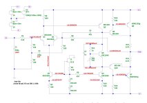
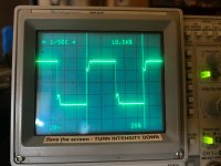
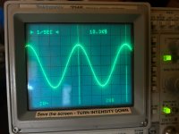
The circuit is the front end of the Pass A-40 with a CFP output stage. Powering up with VR1 all the way up, all the voltages match per the LTSpice sketch. However, once I touch the output with the signal generator positive (or any metallic object) the bias current jumps 500mA. The output sine wave is thick and zooming in shows a 4Vp-p 4MHz clean sine wave.
Apart from being fat, the output sine wave is normal as the level and frequency is changed. This is the same with any changes to the bias.
Rearranging Q7, Q8, Q9, Q10 to form an EF output stage (with a 150R between Q9e and Q10e) does not change things. However, removing the drivers and connecting Q7b and Q8b directly to the VAS results in a clean sign wave and square wave with no ringing for any bias current. The output is normal with input voltage and frequency changes up until the negative clips at about 10Vp.
I tried base stoppers 4.7 to 10R for all the output transistors. I changed Q5 from a KSA992 to a BD140. I tried KSA1220 and KSC2690 for Q9 and Q10.
The pcb is 100mm square with 4 layers -- signal top & bottom, power on 2 and ground on 3. Output and drivers connected by wires to the pcb, Q7, Q8 on heatsinks with a fan. The grounds from the board to the power supply common goes through a 10R resistor bypassed with a 0.68u Wima. The PS common is lifted from earth, the scope probe ground is not used and the only path to earth is the signal generator negative.
I pretty sure my test setup (3CH PS and signal generator, both Instek) are not the problem because I have built the Hiraga 30W Class A and there were no issues with proper grounding, etc. Appreciate any help or insights as to what I think should be a simple design.
Attachments
How about change it into miller compensation? Remove C4 and add 220p cap on the base and collector of Q5.
CFP output stage needs base stopper to be safe. Add a pair of 100 ohm resistors at the base of the driver transistors.
CFP output stage needs base stopper to be safe. Add a pair of 100 ohm resistors at the base of the driver transistors.
You have a few things there that need attention:
1. Place a coil at the output to prevent high-frequency signals / RF from entering back the amplifier (c2 not required with your amp):

2a. Reduce the wire loom length:
3. You have ground fill and what seems to be a Vcc fill... but you do not talk about power supply rail decoupling by means of a 0.01-0.47uF capacitor. FW amps do not use these caps - that doesn't mean that the amps actually do not require them!
4. Stopp doing this... (below):
Tune components in 1. and in 3. with the actual speaker wires connected to the amp output; simulate the load with a resistor and capacitor in parallel. Do not subject an amp to conditions/poking, that will not present themselves in real life. However, DO use a combination of the resistive and capacitive loads at the end of speaker wires... (include the speaker wires).... and then ensure amp stability.
Good luck
1. Place a coil at the output to prevent high-frequency signals / RF from entering back the amplifier (c2 not required with your amp):
2a. Reduce the wire loom length:
2b. Show us the photo of the built ampOutput and drivers connected by wires to the pcb
3. You have ground fill and what seems to be a Vcc fill... but you do not talk about power supply rail decoupling by means of a 0.01-0.47uF capacitor. FW amps do not use these caps - that doesn't mean that the amps actually do not require them!
4. Stopp doing this... (below):
... measure/play with the amp with the actual speaker wires connected to its output.once I touch the output with the signal generator positive (or any metallic object) the bias current jumps 500mA
Tune components in 1. and in 3. with the actual speaker wires connected to the amp output; simulate the load with a resistor and capacitor in parallel. Do not subject an amp to conditions/poking, that will not present themselves in real life. However, DO use a combination of the resistive and capacitive loads at the end of speaker wires... (include the speaker wires).... and then ensure amp stability.
Good luck
Also you need a resistor in front of C1 to form an RC input filter. I normally set the cutoff frequency to be around 200kHz, but other designers have different ideas.
I am currently restoring an Eico HF-81. The AUX channels are working fine, but I am having an issue with one of the PHONO channels. One of the phono channels is intermittent - sometimes it works and (more often) it doesn't. When it is working it, it is a considerably lower volume than the other channel. I've tried swapping tubes and the RCA connectors and neither has made a difference. This morning I powered it on and the channel was working, although quieter than the other. I switched the input selector knob, and when I went back to phono the channel was out. I gave the switch a good clean with Deoxit, but still no luck. I'm going to check for bad solder joints. Anything else I should consider or check?The circuit is the front end of the Pass A-40 with a CFP output stage. Powering up with VR1 all the way up, all the voltages match per the LTSpice sketch. However, once I touch the output with the signal generator positive (or any metallic object) the bias current jumps 500mA. The output sine wave is thick and zooming in shows a 4Vp-p 4MHz clean sine wave.
Apart from being fat, the output sine wave is normal as the level and frequency is changed. This is the same with any changes to the bias.
Rearranging Q7, Q8, Q9, Q10 to form an EF output stage (with a 150R between Q9e and Q10e) does not change things. However, removing the drivers and connecting Q7b and Q8b directly to the VAS results in a clean sign wave and square wave with no ringing for any bias current. The output is normal with input voltage and frequency changes up until the negative clips at about 10Vp.
I tried base stoppers 4.7 to 10R for all the output transistors. I changed Q5 from a KSA992 to a BD140. I tried KSA1220 and KSC2690 for Q9 and Q10.
The pcb is 100mm square with 4 layers -- signal top & bottom, power on 2 and ground on 3. Output and drivers connected by wires to the pcb, Q7, Q8 on heatsinks with a fan. The grounds from the board to the power supply common goes through a 10R resistor bypassed with a 0.68u Wima. The PS common is lifted from earth, the scope probe ground is not used and the only path to earth is the signal generator negative.
سعر الذهب في الامارات
I pretty sure my test setup (3CH PS and signal generator, both Instek) are not the problem because I have built the Hiraga 30W Class A and there were no issues with proper grounding, etc. Appreciate any help or insights as to what I think should be a simple design.
Anyone have any experience replacing the input selector switch on these?
Probably, agreeHow about change it into miller compensation? Remove C4 and add 220p cap on the base and collector of Q5.
CFP output stage needs base stopper to be safe. Add a pair of 100 ohm resistors at the base of the driver transistors.
little impedance anywhere from 33 to common 100 ohms will do at the driver base.
Since the board doesn't have them, think most the problem is the compensation type.
Actually will get strange peaks and phase behavior if the value is too high.
Same weird behavior I have seen driving diamonds with opamps. Big peak around 7 MHz in this case with sim
likely explain the 4 MHz being observed with real devices.

Appreciate any help or insights as to what I think should be a simple design.
Looking at a sim with exact devices shown in post #1 attachment.
Q5 is about 6ma of current, I would take it up to 8ma for a BD140 by changing R10 to 82 ohms instead of 100 ohms.
Drivers Q9 and Q10 also dont have enough current with R15/16 being so high at 240 ohms
R15/16 should be lowered to 120 to 150 ohms.
C4 seems to be to high at 47p lower to 22p to 27p
With these changes in sim, seems to remove all the phase issues noted above
which showed around 7 MHz likely your 4 to 5 MHz with real devices.

Last edited:
I don't see a Zobel network in the diagram. @Extreme_Boky mentions an output coil. Yes 👍
This looks similar (ish) to Rod Elliots P3 and that would be unstable configured as yours is. The 100pf is missing in the sim. Unstable:


This looks similar (ish) to Rod Elliots P3 and that would be unstable configured as yours is. The 100pf is missing in the sim. Unstable:
C6 usually not needed if the amp does not have excessive DC offset and the driver current is high enough.
Plus base resistors to the drivers and a small cap across the VBE
Rods amp will have excessive DC offset at least for CFP, not enough driver current and nothing in the
VBE to help it. C6 is very much needed but goes away, with correct currents and even degen in numerous places.
Was surprised how stable the modified A40 with CFP was.
But agree is likely not suitable for compensation used.
Or could be perfected better and would allow less Cdom for better slew at high frequency
using a combination of the 2
Real life we dont know if this board has decoupling very very close to the output devices since it is also important.
Last edited:
That was the problem -- the compensation cap needed to be hooked to Qb5.How about change it into miller compensation? Remove C4 and add 220p cap on the base and collector of Q5.
CFP output stage needs base stopper to be safe. Add a pair of 100 ohm resistors at the base of the driver transistors.
I measure 7.2mA at R10 (100R). Go for higher?Looking at a sim with exact devices shown in post #1 attachment.
Q5 is about 6ma of current, I would take it up to 8ma for a BD140 by changing R10 to 82 ohms instead of 100 ohms.
Zobel on the pcb as well as rail caps, 100pb welded across Q10b-c as in the picture. The instability stopped when C4 was changed. Base stoppers were added also.I don't see a Zobel network in the diagram. @Extreme_Boky mentions an output coil. Yes 👍
This looks similar (ish) to Rod Elliots P3 and that would be unstable configured as yours is. The 100pf is missing in the sim. Unstable:
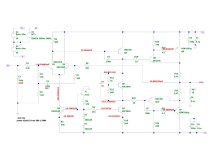
Thank you all for the responses -- I am quite new at solid state amp builds and took this on as a learning experience and your help is greatly appreciated. Right now the prototype is stable and will soon test with speakers. The pcb is configured per the attached LTSpice sketch. The pcb was originally for a Pass A-40. Making a clean board with the suggestions above. The board below has the following readings with 24V rails:
-- DC offset 11mV
-- Frequency response to 48kHz (where output voltage begins to fall)
-- Any bias from a few mV to 1.2A holds steady
-- Stable into a 4-ohm load (power resistor)
Attachments


- Home
- Amplifiers
- Solid State
- Problem with HF on Amplifier Output Signal