I have a ANK DAC 4.1, which uses a CS814=>AD1865 implementation.
The cheap USB input board failed, so I was planning to replace it with the XMOS based I2SoverUSB board.
But I also thought.. since I am at it, why not replacing the whole DAC board with a XMOS => AD1862 implementation.
The new design would use dedicated separated supplies for the digital and analog sections, and the outputs of the DAC chips would be directly connected to the I/V transformers that drive the original tube output stage, as per original audio note design.
Long story short.. anyone who has experience playing with the AD1865 and AD1862 would suggest one over the other?
Thanks,
Marco
I vote for 62 - I was born this year 🙂
Seriously, of all the ancient DACs, the AD1862 is my favorite.
Alex.
Seriously, of all the ancient DACs, the AD1862 is my favorite.
Alex.

The 20-bit AD1862 was the pinnacle of Analog Devices multi-bit DAC range. The 18-bit AD1865 was just under it. Also, the 1862 is a mono DAC requiring two chips for stereo, while the 1865 is a stereo chip containing dual DACs. Which sounds better, as always, is a matter of opinion.
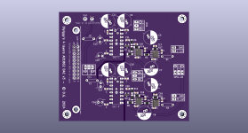
I gave here an AD1862 pcb inspired from the miro1360's work by redesigning the analog aera to feed the DAC analog section and the double op amp section (I/V ( inverted input)+ buffer (non inverted input) with own PS supply section. the digital section has its on PS plug as well, so needs 3 power supplies. (+5V,+12V+op amps stage)
The original pcb is already embedding an header to plug the I2Sover USB board as well as uf-l sockets. It is cheap to print as it is two layers (I have also a more refined 4 layers one design but not public domain, though cheap)
Diyyigy's tribute to miro1360 AD1862 's DAC : gerbers of the 2 layers packaged for JLCPCB.
Edit: here a picture of the 4 layers (top has an header for the I2SoverUSB board and uf-l pads are at the bottom. This 4 layers was made for my needs, no crossing currents, impedance matching, forced path for current by playing with some isolation and the layers with the trough holes... works with VFA as well as CFA for the I/V and permits find op amps settuping compensation, etc... Board is 9.5 cm x 8 cm)
Attachments
Last edited:
Thank you all for the suggestions! It seems like the AD1862 is an indiscussed winner.
@diyiggy's implemenation looks great with the direct connection to the I2Sover USB board and 3 independent power domains.
Would you mind sharing the Kicad file so I can create a variation without the output op-amps?
@diyiggy's implemenation looks great with the direct connection to the I2Sover USB board and 3 independent power domains.
Would you mind sharing the Kicad file so I can create a variation without the output op-amps?
AD1862 is mono DAC 20bit AD1865 is stereo DAC 18 bit
Probably will be better to have dual mono but from the first point of AD source?
That can be done with 2 x AD1862 but deserves dual independent power suplies, digital isolation from pure digital domain.
Probably will be better to have dual mono but from the first point of AD source?
That can be done with 2 x AD1862 but deserves dual independent power suplies, digital isolation from pure digital domain.
Thank you all for the suggestions! It seems like the AD1862 is an indiscussed winner.
@diyiggy's implemenation looks great with the direct connection to the I2Sover USB board and 3 independent power domains.
Would you mind sharing the Kicad file so I can create a variation without the output op-amps?
For the 4 layers ? Nope... 200 to 300 hours of work and several protoypes, third itteration there with a lot of tricks. No bad output stages plug-in boards. So if interrested people can buy one pcb for 30 euros (w/o shipping), as I said : not public domain.
The 2 layers is free, has 3 independant PS too, and willl cost you 7 euros to print at JLCPCB for 5 boards, it is cheap because 2 layers only. But one with one op amp only (smd as dip8) exists in the thread (the gerbers I mean). Just op amps layout is simplier to follow what has disscussed in the main thread.
If you are interrested to tube it for instance (no op amp stage), you will find the gerbers of a 2 layers with dip 8 op amps so you can wire for tube outputs or either rewrok the gerbers given here to your own specs, tribute at miro1360 work. Gerbers of one of the version : first post ! But people whom worked with tubes as discret/op amps, prefered the last over tubes whatever it is is triode DHT or classics : look for @woodturner-fran and @grunf as well as @EUVL work.
But I spend so much times on the 4 layers, one will have pain to do bettter imo with at the same time not being closed by anotherone choices for digital front ends and power supplies as care to current return paths which is very tricky, mind you... It is not I want to make monney with that at that price, but understand it costs a lot of time and monney and populated boards to improve it to a point you never saw such itterative work in commercial products. Cause it was for my own obsessiv needs and I have looked at most of the few commmercial itterations from TEAC, Audio Note, etc... poor work on the pcb layout. So if I sell fews units it covers a little of the labor and parts to continue the game !
Anyway if you read the big thread advised above, you will see almmost all has been disscused from the front end to the output stages, you may find your hapyness there w/o reinvent the wheel cause most of the work has been shared. Many people have shared tips (as your servitor), gave pcbs shematic and/or gerbers of output stages, etc : they almost all are listed on the blog of miro1360 which is a great effort of didactic synthesis.links Of course you will find itterations with shift register to get rid of inputs boards like I2SoverUSB. You will see also miro1360 made a cpld (read the blog page), and also some members like @eclipsevl made a clever USB to I2S board for that ICs (and others).
I think this post migth you save a lot of time...
cheers
Last edited:
Hello,
Last batch of the 4 layers pcb is sold, but I can purchase a new set of 5 boards at JLCPCB if you are not hurry (they usually take 15 days in my mailbox)
The 4 layers unpopulated pcb + BOM and shematic is sold 30 euros (PP family) + shipment at cost (registred parcel). If you are hurry, there is a link just above at post #6 for gerbers files of a simplier 2 layers (free use for DIY) for VFA op amps only (the 4 layers layout being ablle to use the CFA AD811 or the TIA op861 as others VFA op amps of course)
Both needs the USB board from JLSOUNDS or I2S to PCM board from Iancanada (via uf-l plugs option at the bottom side for the 4 layers), or @eclipsevl York board via uf-l too with more choice for the crystals parts (reclocker).
Soldering SMD parts is a must. Or I can organise a Group Buy with minimum order quantity if there are interrest for a pre factory soldered boards batch. The littliest smd size are 0805 package capacitors. But I don't think there can be too much interrest for the factory soldered version. This pcb was made for my needs and AD1862 dac chips are not easy to get.
Thanks for your interrest.
- Home
- Source & Line
- Digital Line Level
- AD1862 vs AD1865