Hi All,
I've built the hi-fi headphone amp from Rod Elliott (project 113) and it sounds great (measures very well in LTSpice as well), however, I didn't get around to matching the BD139 and BD140 output transistors. I realise that it's probably unnecessary and doubtful that I'd ever hear a difference, but I decided it would be nice to do.
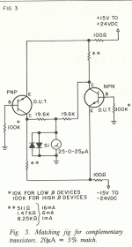
I found a thread (now closed) discussing this in which a matching circuit was offered by kct (I have attached the PDF here, I hope that's OK).
My question is that I have modelled this in LTSpice (attached), and whatever random transistors I pick, I still get well below the suggested 20 ua, so have I done something wrong in my simulation?
I'm sure that LTSpice must deal correctly with transistor gain and from what I understand (not a lot, unfortunately) the circuit appears fine.
So, I'm a bit baffled and left wondering if it's worth building it. Any comments, insights or advice would be very welcome 🙂
I've built the hi-fi headphone amp from Rod Elliott (project 113) and it sounds great (measures very well in LTSpice as well), however, I didn't get around to matching the BD139 and BD140 output transistors. I realise that it's probably unnecessary and doubtful that I'd ever hear a difference, but I decided it would be nice to do.
I found a thread (now closed) discussing this in which a matching circuit was offered by kct (I have attached the PDF here, I hope that's OK).
My question is that I have modelled this in LTSpice (attached), and whatever random transistors I pick, I still get well below the suggested 20 ua, so have I done something wrong in my simulation?
I'm sure that LTSpice must deal correctly with transistor gain and from what I understand (not a lot, unfortunately) the circuit appears fine.
So, I'm a bit baffled and left wondering if it's worth building it. Any comments, insights or advice would be very welcome 🙂
Attachments
Have you considered that Spice models of complementary devices will have equal gain since they are not real devices with real manufacturing spread?
Ah, thanks, that was sort of what I thought might be happening, but I was still surprised that picking random transistors, with presumably different gain ranges, still seemed to work. Even non complementary devices.
That's an interesting circuit, probably works well.
Compliments will never match closely over a current range, but close in some cases beats the heck out of not trying. Like diff pairs, to compare you need to keep the cases at the same temperature exactly.
Compliments will never match closely over a current range, but close in some cases beats the heck out of not trying. Like diff pairs, to compare you need to keep the cases at the same temperature exactly.
Your forgot to check whether both transistors are operating in forward active mode where |Vce| > |Vbe| . With the two device models shown is post #1 and the resistor values shown in post #1, this causes a problem.
The easiest way to see it, is to name every node on the schematic. After running the .OP analysis, manually calculate Vce and Vbe for each transistor. Voila.
It seems like a cumbersome and needlessly fiddly test fixture, if you have to modify the resistor values (using matched pairs of resistors) when you change the Devices Under Test.
Probably you want the ratio (R8 / (R7 parallel R6)) to be far far greater than the beta of the very highest beta transistor you'll test today. Which in the case of post#1 is Beta=650 (!!)
_
Attachments
Last edited:
Hi Mark,
I'd have to build it to be sure, but it does look like both parts are forward biased and conducting. Base current for the PNP is about 14.4 VDC across 100K, similar for the NPN. The collector currents are not defined of course, if equal should give an approximate zero at "Julie". What you really want to do is make the two base currents exactly equal. You could do that by combining R4 with R8 and break the common to ground. That forces equal base currents at whatever test current you choose.
Am I missing something?
Hi Mark, Anntech,
Thanks for your comments. I checked the current in R3 and R7 and found them to be about -3.4 and 3.4 respectively, which suggested to me that the devices were conducting. But perhaps they are not switched on enough? Checking the emitter currents I find PNP to be 4.3 ma and NPN to be -4.3 ma. Does that sound OK?
Anatech, are you suggesting that the bases are joined and there is then a single 100k to ground?
Last edited:
Hi Clockworktent,
That sounds fine. They are both conducting.
No, there should be some resistor between the bases and not connected to anything else (no "ground" connection). Probably 200K to keep the same conditions.
I am waiting to see what Mark might suggest here as well.
That sounds fine. They are both conducting.
No, there should be some resistor between the bases and not connected to anything else (no "ground" connection). Probably 200K to keep the same conditions.
I am waiting to see what Mark might suggest here as well.
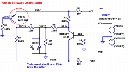
It's all right there in the LTSPICE simulation of post #1. Run it and look at the results. You'll discover that
1. The voltage at the collector of the PNP (node "INDIA") is greater than the voltage at its base (node "HOTEL"). Thus |Vce| < |Vbe| and the PNP transistor is not in forward active mode
2. The collector current of the PNP is 4.18mA and the base current of the PNP is 0.139 mA. The ratio of these two currents, the "current gain", is 30.1 . However the transistor .MODEL specifies that the forward beta of this transistor is 651. Thus the PNP transistor is not in forward active mode.
3. Here is the biggest mistake in this circuit design: the base resistors R4 and R8 are too small. They set the base currents to approx (15 - Vbe)/100k = 140uA. With Beta=650, you expect a collector current of 91 milliamps. 91 milliamps flowing in R3 and/or R7, gives a voltage drop of 751 volts (!) which exceeds the 30 volt power supply considerably. The power supply and the collector resistor, limit the collector current to a value way WAY less than (BaseCurrent x Beta). It's a design error. You could try the resistor ratio suggestion mentioned in post #5 to see whether it cures the problem.
I'll leave the analysis of the NPN half-circuit, as an exercise for the reader. You've got LTSPICE, run it.
_
Attachments
Last edited:
First off, no BD140 will have a beta of 650. BF being set to 650 by itself does not necessarily guarantee a gain of 650 - it depends how much is being scrubbed off at both ends. Depending on settings for Ikf and Ise, you may never peak the beta that high. I had a 2N3773 model with BF at over 300, but never peaked over 80 (and that was around 1 or 2 A). A peak gain of maybe 180 or 200 for the BD140 is possible.
That jig will probably go completely out of whack with severe mismatch, especially with power devices which have different gain profiles vs. IC. If one transistor is cut off and the other on full bore the match is probably pretty bad. Put in closer match into the simulation and it will likely behave a bit better.
That jig will probably go completely out of whack with severe mismatch, especially with power devices which have different gain profiles vs. IC. If one transistor is cut off and the other on full bore the match is probably pretty bad. Put in closer match into the simulation and it will likely behave a bit better.

Hi Mark,
Firstly, don't have a simulator and don't entirely trust them (so no loss to me). I have a sense or understanding for most circuits, and if in doubt for a simple circuit I simply build the thing.
The PNP base-emitter is forward biased. It has to be, there is no choice. Same for the NPN. You can saturate a transistor but the emitter-base is still forward biased.
This jig has issues with some of the resistor values, and that's fine. Build it, see what it does and adjust if necessary. Like all jigs that balance conduction, it won't work well with parts that aren't close. But then, who cares? If I designed it, I would configure it so that the collector-emitter voltage was more constant and around 10 VDC. I hadn't thought of doing something like this and I think it has the seeds of a cool idea.
Hi wg_ski,
Thanks for injecting some reality. Agreed that the expectation for beta is not anywhere close to what you'll find in the real world for those. You've illustrated why depending solely on a simulator is so dangerous. You've also got to pay attention to the models used and check to see if they are realistic.
That's why I just figure it out on paper (makes you think) and then build the darned thing. They usually work with component value tweaks.
Assume beta = 65, 10% of the .MODEL parameter value
Base current = 140uA { (15V - Vbe)/100k }
Collector current = 65 * 140uA = 9100uA = 9.1mA
Voltage dropped across R7 = (9.1mA * 8.25K) = 75 volts
Total supply voltage available = 30 volts
Conclusion: design error
Base current = 140uA { (15V - Vbe)/100k }
Collector current = 65 * 140uA = 9100uA = 9.1mA
Voltage dropped across R7 = (9.1mA * 8.25K) = 75 volts
Total supply voltage available = 30 volts
Conclusion: design error
Hi Mark,
Given it is a general design idea ... You are supposed to adjust values depending on the parts you are testing. Please read the notes in the first attachment, figure 3.
Additionally, you are arguing a simulator. What would you say to someone who built it, followed the directions and had it work properly? Reality beats a simulator hands down every single time. You have got to sit at a bench with parts and a hot soldering iron to actually know anything at all.
My recommendation for how to "adjust values depending on the parts you are testing", appears in post #5 above. Line 4.
Right, so why are you picking it apart?
The concept works, period. I think it shows promise.
You got stuck on the values for a bad model. Why not look for solutions instead of reasons why you think it is a bad design? Pull yourself away from the simulator, acknowledge the real world and work with it.
The concept works, period. I think it shows promise.
You got stuck on the values for a bad model. Why not look for solutions instead of reasons why you think it is a bad design? Pull yourself away from the simulator, acknowledge the real world and work with it.
If it helps, here's a link to the original thread (which is now closed, otherwise I'd have posted there). It might provide some useful context.
Hi,
Anyone to know, How to matching PNP with NPN Transistor?
I buy 2N5551= 20 ea. and 2N5401 = 20 ea. then hFE measure is more difference
hFE of 2N5551 = 110 to 130
hFE of 2N5401 = 210 to 230
I am making the power amplifier, when I put them in the circuit, It may be not good sound.
Have anyone suggestion?
sorry!!! My english is not good.
Senee
- senee
- Replies: 20
- Forum: Solid State
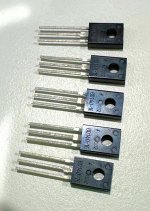
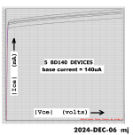
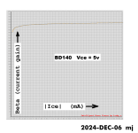
Turns out I've got some Fairchild BD140s in my drawer so I measured five of them on the curve tracer. Beta was right around 175. Not 650 and not 65. Beta was ~ 175. Between the smallest and largest value, the delta was 10% so I guess you could say, plus or minus 5%.
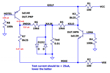
If anyone wants to adapt the original circuit in post #1 to measure these real BD140 devices, I suggest changing the base resistor value (R4 and R8) to about 3.9 megohms. This will give a base current of (15 - 0.6)/3.9E6 = 3.7 microamperes. With a beta of 175, the collector current will be 0.65mA. Then the drop across the collector resistor (8.25k) cannot exceed (6.5E-4 * 8.25E+3) = 5.3 volts, comfortably less than the power supply voltage. So the device remains in the forward active region with plenty of safety margin.
However, if you leave the base resistors R4 and R8 at 0.1 megohm as shown in post #1, you're asking for trouble. The base current will be 39x greater, making the collector voltage shoot up so high that |Vce| < |Vbe| and the device will exit the forward active region.
_
Attachments
Thanks, Mark, it seems that setting R4 and R8 to 3.9 meg solves the problem and the circuit (LtSpice sim) can now differentiate between different transistors.
Interestingly, despite the differences in bf, the BD139 and BD140 in my sim now produce a test current of 11.2 ua, which is what one would hope. Picking random devices now produces much higher test currents. Looks like it will work.
Interestingly, despite the differences in bf, the BD139 and BD140 in my sim now produce a test current of 11.2 ua, which is what one would hope. Picking random devices now produces much higher test currents. Looks like it will work.
Personally, I would adjust values so that the parts were conducting about the same current as they would in the application. Running these parts at such a light base current may not give you the results you hope for.
Always match devices close to the currents you expect them to run at. For outputs that would be the expected idle current.
Always match devices close to the currents you expect them to run at. For outputs that would be the expected idle current.
- Home
- Amplifiers
- Solid State
- Matching NPN and PNP