BRIEFLY: EDA software is the best tool for audio projects but there is a
special use-case for stripboard partitions with easy, compact layouts.
special use-case for stripboard partitions with easy, compact layouts.
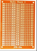
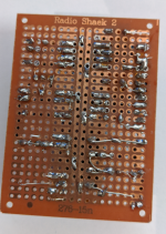
SHAEK-BARE.PNG: I came across this "Shaek" clone of the Radio Shack
276-150 on Amazon when looking for something else. This YUNGUI item
was in Circuit-Breaker-Panels, not electronics. It is not very good
for soldering because the holes are too big for 1/4W resistors and
such. However, the layout is interesting because it has power rails
centered and there is room on each side of DIP sockets for related
resistors. This layout is logical and efficient. Such prototyping
boards are rarely seen now because they are mostly designed as
companions of plastic breadboards with 5-nothing-5 holes and power
strips on the sides.
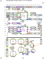
SHAEK-ROUTED.png: Veroroute models vertical/horizontal stripboards but
does not have a model for hybrids. In fact, it can be used for any PCB
structure with standard spacing for holes and vias. A circuit can be
"painted" manually but I use the autorouter and add symbolic wires or
pads when auto does not go my way. I add a row of pads at the top to
mark how the strips are partitioned. Non-functional circle-X symbols
help to trace track alignment. See SB-ROUTED for more details.
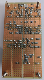
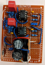
SHAEK-TOP.png: I wired a small HeadAmp with two opamps plus linear
power supply(+/-12vdc) on the Shaek board. Everything fit when
planned using Veroroute. A headphone test revealed a rising high
frequency response probably from the unshielded external volume
control wires. A 100pf cap to ground pin 3 of the 4556 can produce
normal sound. The stripboard version has this fix. See SB-TOP.
SHAEK-WIRES: The holes are too big for the resistor pins. I had to
bend component pins to insure connection before soldering. There are no
interconnect wires on the copper side.
STRIP-LARGE.png: Stripboard or Veroboard has long, parallel strips of
copper which must be cut and/or bridged to create circuits for
electronic devices. This is easy for trivial circuits but becomes
difficult as complexity increases. Circuit tracks must be cut
(Carefully) with a 5/32 drill bit or sharp knife. It is easier, using
the Radio Shack pattern, to make vertical cuts (for partitions) across
all the tracks at once with a fresh hacksaw blade. See SB-WIRES and
SB-ROUTED.
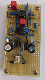
SB_TOP.png: I was inspired by .Douglas.Self:Small Signal Audio Design'
chapter one which had a low impedance drive for tone control
circuits. It was not in the headphones chapter but it can drive them
with a suitable opamp such as 4556. Since the 4556 version merges gain
and buffer functions, there is no need for another opamp gain
stage. This is about using stripboard partitions, so a small but
usable circuit is satisfactory for demonstration.
SB_WIRES.png: First a 19-hole section was cut from a wide
stripboard. Then the copper was gently cut vertically with a fresh
blade to reveal two strips for the DIP sockets and separate strips for
the adjacent components. So there are four partitions. There are a few
spots where a copper cut is not desired and a jumper is installed to
"uncut" it. But this is less complicated than making random cuts on a
large stripboard. And stray capacitance should be reduced. There are
no wires on the copper side and the top wires are perpendicular to the
tracks for minimal coupling.
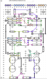
SB_ROUTED.png:
I add a row of pads at the top to mark how the strips are partitioned.
There are copper cuts at 4, 10, and 15. Non-functional circle-X
symbols help keep track of the vertical copper cuts.
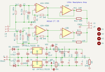
HA-LITTLE.png: KiCad Schematic of "mother's little helper". There is a
schematic note "added C7,C8" to remedy spurious feedback or
instability from my crude setup wiring.
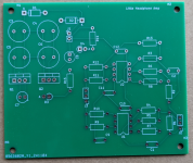
KI-PCB.png: Simple 2-layer layout of HA-LITTLE. There was a problem in
my routing attempt where I needed to use a via but could not get that
to work even after I watched a video where it was easy. So I redid the
routing to work with only two layers.
,,,
Attachments
-
 HA-LITTLE.png55.5 KB · Views: 52
 -
 KI-PCB.png596.4 KB · Views: 43
 -
 SB-ROUTED.png126.4 KB · Views: 48
 -
 SB_TOP.png596.7 KB · Views: 50
 -
 SB_WIRES.png688.1 KB · Views: 54
 -
 SHAEK-BARE.png141 KB · Views: 52
 -
 SHAEK-ROUTED.png114.7 KB · Views: 52
 -
 SHAEK-TOP.png676.7 KB · Views: 53
 -
 SHAEK-WIRES.png455.5 KB · Views: 51
 -
 STRIP-LARGE.png74.9 KB · Views: 52

Here's what I use for quick breadboarding.
https://www.pcbway.com/project/shareproject/W31870ASS4_PPH100sq.html
It's a variation of one of Vector's old designs (still available but way expensive). But you can order 10 of them fairly inexpensively from PCBway, to keep around for quick builds.
Pad per hole on 0.1inch (2.54mm) spacings with solid ground plane on reverse side. Pads are isolated from ground, but you can just solder a lead from a pad to the plane to ground it. Good isolation and shielding. And if you do any RF work, a line of the pads tied together makes a fairly decent 50ohm microstrip line for up into UHF frequencies.
A ground plane is good to have. Are there any builds to demonstrate these boards. I would be concerned about short circuits.Here's what I use for quick breadboarding.
https://www.pcbway.com/project/shareproject/W31870ASS4_PPH100sq.html
It's a variation of one of Vector's old designs (still available but way expensive). But you can order 10 of them fairly inexpensively from PCBway, to keep around for quick builds.
Pad per hole on 0.1inch (2.54mm) spacings with solid ground plane on reverse side. Pads are isolated from ground, but you can just solder a lead from a pad to the plane to ground it. Good isolation and shielding. And if you do any RF work, a line of the pads tied together makes a fairly decent 50ohm microstrip line for up into UHF frequencies.
Ive done dozens of ckts on these. The holes are spaced from plating by a bare ring, no chance of unintended shorts to ground. But plane -side part leads can reach ground easily when you need, with a small solderblob bridge. Put the parts on the plane side, leads thru to the pads.
Ive also done SOIC ckts. (slicing pads in half with razor hobby knife), works pretty well.
Sorry, no photos at hand, but shorts aren't an issue any more than with typical pad-per-hole boards
(It's like a Vector 3007).
Ive also done SOIC ckts. (slicing pads in half with razor hobby knife), works pretty well.
Sorry, no photos at hand, but shorts aren't an issue any more than with typical pad-per-hole boards
(It's like a Vector 3007).
Last edited: