Hi,
I'm making a multilayer DAC pcb.
I have a 50 mils slot between Agnd & DGND.
On one of the pcb edge I have a resistor after a 1 mH coil that bridge the power planes of each side. It is for distributing some power to a batch of digital ic, flip flops.... on the digital side of the pcb this distributed power plane has almost no reference use for signal, but as a ground return path for a reference layer where smd caps end.
I am worrying about that slot for the current return path towards the PS.
Should I continue a reference plane on a layer till the plarity of that power supply smoothing cap near the secondary ? just on the half part of the smoothing cap below the power plane of that polarity ?
that reference return path is independant of the others reference layers, so not coupled by via fencing for instance.
Or does the current will jump straigth that 50 mils slot gap ?
Or a stitching cap of say 100 nF across the 50 mils gap near the bride resistor is another feasible way for the return current path , bridging an AGND to a DGND ground layers ?
Thanks
What will the clock frequency be for this dac? Can you show the layout you have so far?
Obviously, the AGND and DGND have to be connected at the dac. However, you do have other circuitry on one PCB fiberglass board that would be equivalent to a separate board with some spacing in between the two boards?
You can get away with more if using 5/6MHz clocks and slow-ish risetimes. If using 100MHz clocking that would be a very different matter.
Last edited:
Chapter 17 of Henry Ott, "Electromagnetic Compatibility Engineering" will be helpful to you. Basically, Ott argues that the best performance is obtained with one solid ground plane (i.e., no separate analog and digital ground) as long as the return path for the digital signals is only in the digital part of the ground plane.
Another common solution is to bridge the two planes under the DAC. But you still have to make sure that no return path cross the moat.
Tom
Another common solution is to bridge the two planes under the DAC. But you still have to make sure that no return path cross the moat.
Tom

Hi,
22/24 XOs.
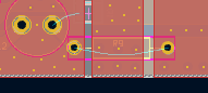
For some reason the Whole ground plane is not feasible for that IC TDA1541A where the power supply of the digital part and analog side is not splitted really, the slot was the best strategy here.
The two ref planes are already bridged at the dgnd pin. I have also two signals traveling through that slot via a resistor for each line with two stitching cap for any return path across the slot near the resistors. (I don't know if they spread back through the DGND pin through the sources, so the stitching caps here are safer)
The 5V I want to distribute comes from a common LM317 that feed a pin of the DAC that is not really digital or analog digital but serves both purpose into the DAC. and another line from that LM317 is going to the power plane of the digital side where the flip flop are. As being near the edge,no problemo to continue a dgnd layer here w/o impacting the AGND ref layers that could on another story.
I could have a ground layer that follows from the digital side to the common smoothing cap is feasible, but anyway the return current doesn(t cross the digitals signals decoupled on another clean reference layer.
On the picture this is the left slot (plain slot on 4 layers (not the other one at rigth where it is DGND aera). The bridgin resistor that distributes the +5V is the one after the L2 coil (1mH)
22/24 XOs.
For some reason the Whole ground plane is not feasible for that IC TDA1541A where the power supply of the digital part and analog side is not splitted really, the slot was the best strategy here.
The two ref planes are already bridged at the dgnd pin. I have also two signals traveling through that slot via a resistor for each line with two stitching cap for any return path across the slot near the resistors. (I don't know if they spread back through the DGND pin through the sources, so the stitching caps here are safer)
The 5V I want to distribute comes from a common LM317 that feed a pin of the DAC that is not really digital or analog digital but serves both purpose into the DAC. and another line from that LM317 is going to the power plane of the digital side where the flip flop are. As being near the edge,no problemo to continue a dgnd layer here w/o impacting the AGND ref layers that could on another story.
I could have a ground layer that follows from the digital side to the common smoothing cap is feasible, but anyway the return current doesn(t cross the digitals signals decoupled on another clean reference layer.
On the picture this is the left slot (plain slot on 4 layers (not the other one at rigth where it is DGND aera). The bridgin resistor that distributes the +5V is the one after the L2 coil (1mH)
Attachments
I think we need to see the whole thing in context, not just a close up of a small area. That said, it may work with what you are doing but it may never be emissions compliant.
Basically, I think Tom gave some good advice. Think about were currents will flow, which may take some getting used to but its probably worth the effort. I wrote a little about the idea at: https://www.diyaudio.com/community/threads/return-to-zero-shift-register-firdac.379406/post-7830183 Also, if you look at some of my layouts you can see how I am trying to make sure currents mostly go where I want them to go. If you do it well, there is much less need for segmentation on all layers. My ground plane on layer 2 is usually continuous, even if some of the surface fill isn't.
Basically, I think Tom gave some good advice. Think about were currents will flow, which may take some getting used to but its probably worth the effort. I wrote a little about the idea at: https://www.diyaudio.com/community/threads/return-to-zero-shift-register-firdac.379406/post-7830183 Also, if you look at some of my layouts you can see how I am trying to make sure currents mostly go where I want them to go. If you do it well, there is much less need for segmentation on all layers. My ground plane on layer 2 is usually continuous, even if some of the surface fill isn't.
Thanks,
I willl look at it.
Basic question, does current of PS (low frequency) can travel trough an empty space of 50 mils, or does it need a substrate ? What are saying Maxwell ? As i have no electrical education but few book...
I also can split it : a dedicated +5V on the DGND side.
I willl look at it.
Basic question, does current of PS (low frequency) can travel trough an empty space of 50 mils, or does it need a substrate ? What are saying Maxwell ? As i have no electrical education but few book...
I also can split it : a dedicated +5V on the DGND side.
you mean with the cap aside the resistor in order the current can flow back here ? (yup no signals there, just supply path, the two AGND DGND meets at the opposite diretion on the top edge of the pcbAnother common solution is to bridge the two planes under the DAC. But you still have to make sure that no return path cross the moat.
Tom
Also, if you look at some of my layouts you can see how I am trying to make sure currents mostly go where I want them to go. If you do it well, there is much less need for segmentation on all layers. My ground plane on layer 2 is usually continuous, even if some of the surface fill isn't.
Yes I agree, but that IC is a b...ch, btw I adapt a shematic made T. Loesch,but I have some pain at following him (his answers are not direct answers so I have to imagine one part of the answer... not easy. I had no pain to make an AD1862 4 layers DAC, but that chip has a common powersupply and return current path may be both analog and digital on some pins (and here anyway the whole bottom layer as an unique reference with two others plan on another layer that meet just at DGND pin is what I wanted to do but I had a no-no when I talked about that. He know that ic alost as his pockets.
Capacitively it can depending on frequency and capacitance. Where you can get into more trouble though, sometimes running a signal across that gap can make the board into a slot antenna, which will then cause it to radiate RFI. There will also be significant reflections if the risetime is fast.Basic question, does current of PS (low frequency) can travel trough an empty space of 50 mils...
What I would suggest to have a digital voltage regulator on the digital side in bring in external power for it only on the digital side. Do similar things on the analog side so that return currents will go back to their own voltage regulator as much as possible.
Also try not to run any signals across the gap if you can help it.
I need to re read the basic, not so much good book fo that basics of what electricity is : AC DC, frequencies, inductance, resistance and capacitance behavior; I studied as an enthusiast but each time for different behavior : illistration : capacitor for filters, etc !
But anyway for him my pcb seems ok, and I'm painting the lily here (cause here not needed in that particular shematic, frequencies involved, etc)
Thanks again both of you for the kind advices anyway ! 🙂
But anyway for him my pcb seems ok, and I'm painting the lily here (cause here not needed in that particular shematic, frequencies involved, etc)
Thanks again both of you for the kind advices anyway ! 🙂
No. I mean joining the AGND and DGND planes under the DAC. No resistor. No capacitor.you mean with the cap aside the resistor in order the current can flow back here ?
Have a look at the CS4398 reference design for an example where all grounds go to the same two copper pours (top and bottom layer): https://statics.cirrus.com/pubs/rdDatasheet/CDB4398.pdf
Tom
And if you can't help running signals across the moat, run them across where the two grounds are bridged.Also try not to run any signals across the gap if you can help it.
Tom
No. I mean joining the AGND and DGND planes under the DAC. No resistor. No capacitor.
Have a look at the CS4398 reference design for an example where all grounds go to the same two copper pours (top and bottom layer): https://statics.cirrus.com/pubs/rdDatasheet/CDB4398.pdf
Tom
Yes I did it like that , bridged at a pin under the ic; The resistor is bridging just power towards a "digital" power plane after the moat on the digital side. The designer said that the frequencies involved are so low and LCRC filtered (the R bridge above the moat, but doesn't join the reference layers (that is done under the ic as said) that no problemo.
Thanks for the link.
OK. So you're not asking about how to bridge the ground planes then? What you're asking is how to best power the analog and digital from the same supply?The resistor is bridging just power towards a "digital" power plane after the moat on the digital side.
Hmmm... But these are digital signals, no? Without any special tricks, digital signals have pretty high edge rates -> lots of high-frequency content. Be careful where you dump that energy.The designer said that the frequencies involved are so low and LCRC filtered
One way to address this is to add some series resistance on the digital lines. That slows the edge rate, but can be costly in terms of jitter depending on the type of digital input the signal goes into.
Tom
OK. So you're not asking about how to bridge the ground planes then? What you're asking is how to best power the analog and digital from the same supply?
Yup ! about potential return path if needed (or not), that's why I asked about stitching capacitors.Another solution I had is to continue the DGND following an edge of the board on a part of that "analog" power. But finally it seems not to be a problem no return path exists when low frequency is involved.
That is what didd the designer : a resistor that bridged the moat with no return path beneath where the moat/slot is (50 mils gap), before is a coil and after an another bulky cap (CLRC filtering).
Te two digital signal lines are delayed bit clock lines comming from a flipflop, they bridge also the moat trough a resistor (and no return path), they input in the dac ic. maybe the pin of the ic where agnd and dgnd bridge makes a return path, but the designer said they treated as dif lines with slow rise time, something like that . I am not acurate in the words as it is above my head. But I do know (no punn intented) the higher the frequency, so the faster the signal, the return path of current will follow back the signal line to the source....
I think I'm lost between the concepts of frquencies involved and Voltage/current, and if AC or DC... Hence the strange questions I surmise.
Last edited:
I personally wouldn't power the analog and the digital from the same power supply. Separate power transformer windings, and separate regulators. More like the following but with two positive power supplies only tied together where the ground planes meet under the dac chip: https://www.diyaudio.com/community/...our-tweaks-mods-and-hints.335881/post-7833163 One external digital supply, and one for analog. Then local secondary regulators on the board as needed.
Of course this isn't the cheapest way but it tends to help the sound.
Of course this isn't the cheapest way but it tends to help the sound.
Well I am a lot in the curiosity phase understantment, cause the designer who is T Loesch you know, seems to know very well what he did with that chip and electronic in general (AMR, Ifi...). But I like to learn (what he helps to btw, but sometimes I have to dig more to understand really... I should go back to the "good" books ; I read tons on pdfs from several years but I am not sure it is efficient when the bases are not well understood enough and learned well...)
I should have the ARt of electronic somewhere, Ott too( thouf=gh it is advanced level already).
I should have the ARt of electronic somewhere, Ott too( thouf=gh it is advanced level already).
This may help alsoHi,
I'm making a multilayer DAC pcb.
I have a 50 mils slot between Agnd & DGND.
On one of the pcb edge I have a resistor after a 1 mH coil that bridge the power planes of each side. It is for distributing some power to a batch of digital ic, flip flops.... on the digital side of the pcb this distributed power plane has almost no reference use for signal, but as a ground return path for a reference layer where smd caps end.
I am worrying about that slot for the current return path towards the PS.
Should I continue a reference plane on a layer till the plarity of that power supply smoothing cap near the secondary ? just on the half part of the smoothing cap below the power plane of that polarity ?
that reference return path is independant of the others reference layers, so not coupled by via fencing for instance.
Or does the current will jump straigth that 50 mils slot gap ?
Or a stitching cap of say 100 nF across the 50 mils gap near the bride resistor is another feasible way for the return current path , bridging an AGND to a DGND ground layers ?
Thanks
https://www.analog.com/en/resources/analog-dialogue/articles/grounding-again.html
G²
There are some excellent videos on YouTube about mixed-signal PCB design from Altium Academy. They are very thorough, complete, and technically accurate. They also mirror some of Tom's excellent comments. Most videos are presented on a whiteboard with hand drawings and don't reference Altium at all!
Most of the stuff online and in books is for high speed digital design. 24-bit data converters are one of the hardest mixed signal designs to get right, at least according to one of those "expert" videos. With 22/24MHz clocks, it turns out the digital and the analog sections may need to be approached rather differently for best results.
- Home
- Design & Build
- Electronic Design
- Stitching capacitor across a slot for current return path